MAX4561_V1 データシートの表示(PDF) - Maxim Integrated
部品番号
コンポーネント説明
一致するリスト
MAX4561_V1 Datasheet PDF : 11 Pages
| |||
±15kV ESD-Protected, Low-Voltage,
SPDT/SPST, CMOS Analog Switches
(TA = +25°C, unless otherwise noted.)
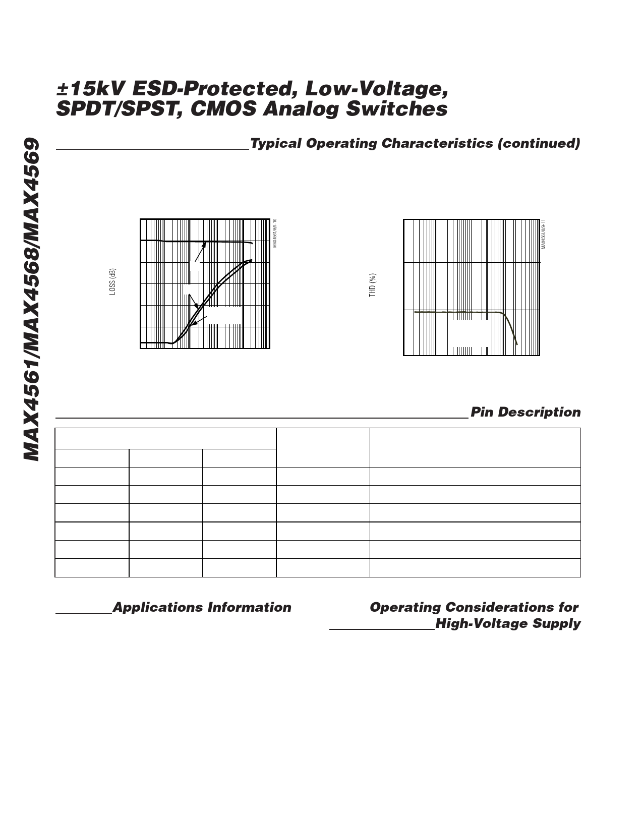
Typical Operating Characteristics (continued)
FREQUENCY RESPONSE
20
0
-20
ON
-40
OFF
-60
CROSSTALK
MAX4561
-80
-100
0.01 0.1
1
10 100 1000
FREQUENCY (MHz)
TOTAL HARMONIC DISTORTION
vs. FREQUENCY
1
0.1
0.01
0.001
10
600Ω IN and
OUT
V+ = 5V
100
1000 10,000
FREQUENCY (Hz)
100,000
MAX4561
1
2
3
4
5
6
PIN
MAX4568
4
5
3
–
1
2
MAX4569
4
5
3
2
1
–
NAME
IN
V+
GND
NC
COM
NO
Pin Description
FUNCTION
Logic Control Input
Positive Supply Voltage
Ground
Analog Switch Normally Closed Terminal
Analog Switch Common Terminal
Analog Switch Normally Open Terminal
Applications Information
Do not exceed the absolute maximum ratings because
stresses beyond the listed ratings may cause perma-
nent damage to the device.
Proper power-supply sequencing is recommended for
all CMOS devices. Always sequence V+ on first, fol-
lowed by the logic inputs, NO/NC, or COM.
Operating Considerations for
High-Voltage Supply
The MAX4561/MAX4568/MAX4569 are capable of
+12V single-supply operation with some precautions.
The absolute maximum rating for V+ is +13V (refer-
enced to GND). When operating near this region,
bypass V+ with a 0.1µF min capacitor to ground as
close to the device as possible.
6
Share Link: 