M312L2828ET0 データシートの表示(PDF) - Samsung
部品番号
コンポーネント説明
一致するリスト
M312L2828ET0 Datasheet PDF : 23 Pages
| |||
256MB, 512MB, 1GB Registered DIMM
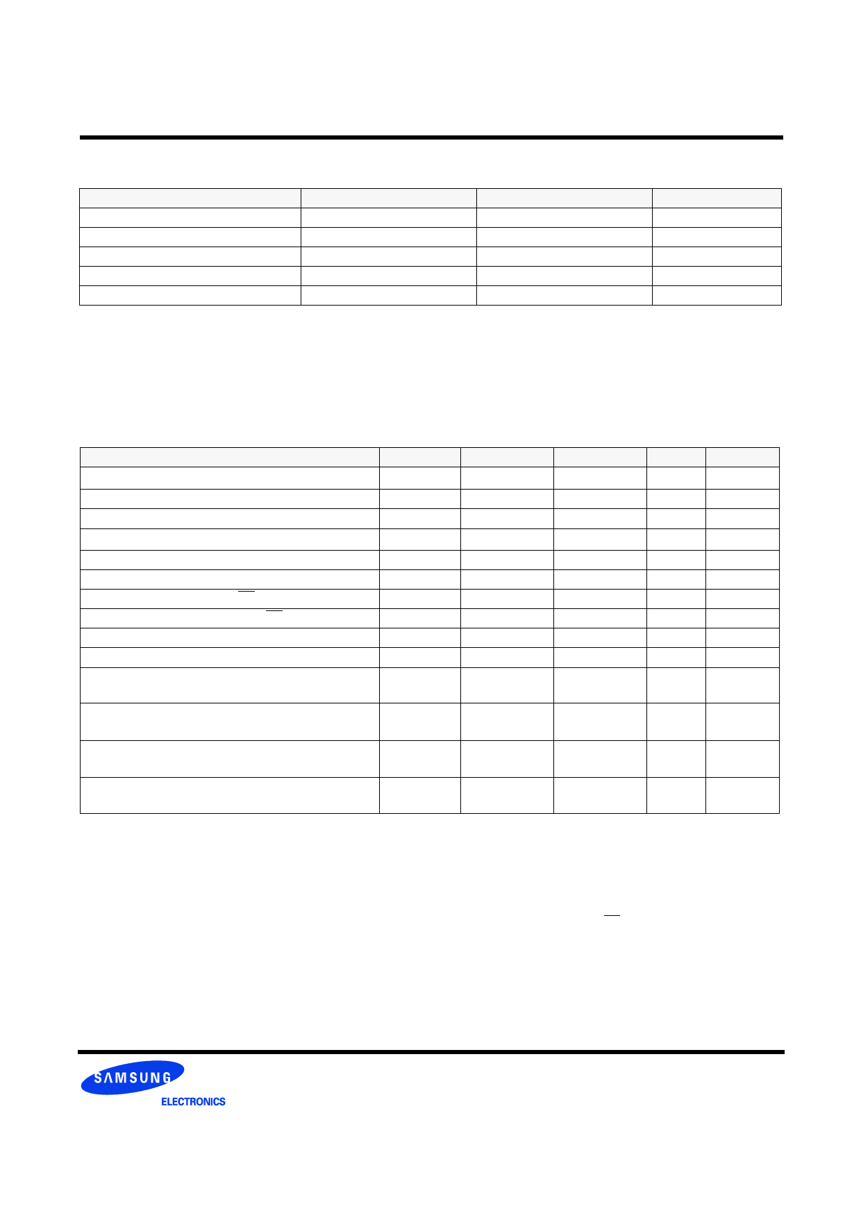
Absolute Maximum Ratings
Parameter
Voltage on any pin relative to Vss
Voltage on VDD supply relative to Vss
Storage temperature
Power dissipation
Short circuit current
Symbol
VIN, VOUT
VDD,VDDQ
TSTG
PD
IOS
DDR SDRAM
Value
Unit
-0.5 ~ 3.6
V
-1.0 ~ 3.6
V
-55 ~ +150
°C
1.5 * # of component
W
50
mA
Note : Permanent device damage may occur if ABSOLUTE MAXIMUM RATINGS are exceeded.
Functional operation should be restricted to recommended operating condition.
Exposure to higher than recommended voltage for extended periods of time could affect device reliability.
Power & DC Operating Conditions (SSTL_2 In/Out)
Recommended operating conditions (Voltage referenced to VSS=0V, TA=0 to 70°C)
Parameter
Symbol
Min
Max
Unit
Supply voltage(for device with a nominal VDD of 2.5V)
VDD
2.3
2.7
I/O Supply voltage
I/O Reference voltage
VDDQ
VREF
2.3
2.7
V
VDDQ/2-50mV VDDQ/2+50mV
V
I/O Termination voltage(system)
Input logic high voltage
VTT
VREF-0.04
VREF+0.04
V
VIH(DC)
VREF+0.15
VDDQ+0.3
V
Input logic low voltage
VIL(DC)
-0.3
VREF-0.15
V
Input Voltage Level, CK and CK inputs
Input Differential Voltage, CK and CK inputs
Input leakage current
VIN(DC)
-0.3
VDDQ+0.3
V
VID(DC)
0.3
VDDQ+0.6
V
II
-2
2
uA
Output leakage current
IOZ
-5
5
uA
Output High Current(Normal strengh driver)
;VOUT = VTT + 0.84V
IOH
-16.8
mA
Output High Current(Normal strengh driver)
;VOUT = VTT - 0.84V
IOL
16.8
mA
Output High Current(Half strengh driver)
;VOUT = VTT + 0.45V
IOH
-9
mA
Output High Current(Half strengh driver)
;VOUT = VTT - 0.45V
IOL
9
mA
Note
1
2
4
4
3
Notes : 1. Includes ± 25mV margin for DC offset on VREF, and a combined total of ± 50mV margin for all AC noise and DC offset on
VREF, bandwidth limited to 20MHz. The DRAM must accommodate DRAM current spikes on VREF and internal DRAM noise
coupled to VREF, both of which may result in VREF noise. VREF should be de-coupled with an inductance of ≤ 3nH.
2. VTT is not applied directly to the device. VTT is a system supply for signal termination resistors, is expected to be set equal to
VREF, and must track variations in the DC level of VREF
3. VID is the magnitude of the difference between the input level on CK and the input level on CK.
4. These parameters should be tested at the pin on actual components and may be checked at either the pin or the pad in
simulation. The AC and DC input specifications are relative to a VREF envelop that has been bandwidth limited to 200MHz
Revision 1.4 February, 2004
Share Link: 