M312L2920BG0-A2 データシートの表示(PDF) - Samsung
部品番号
コンポーネント説明
一致するリスト
M312L2920BG0-A2 Datasheet PDF : 18 Pages
| |||
1GB, 2GB Registered DIMM
DDR SDRAM
184Pin Registered DIMM based on 512Mb B-die FBGA (x4, x8)
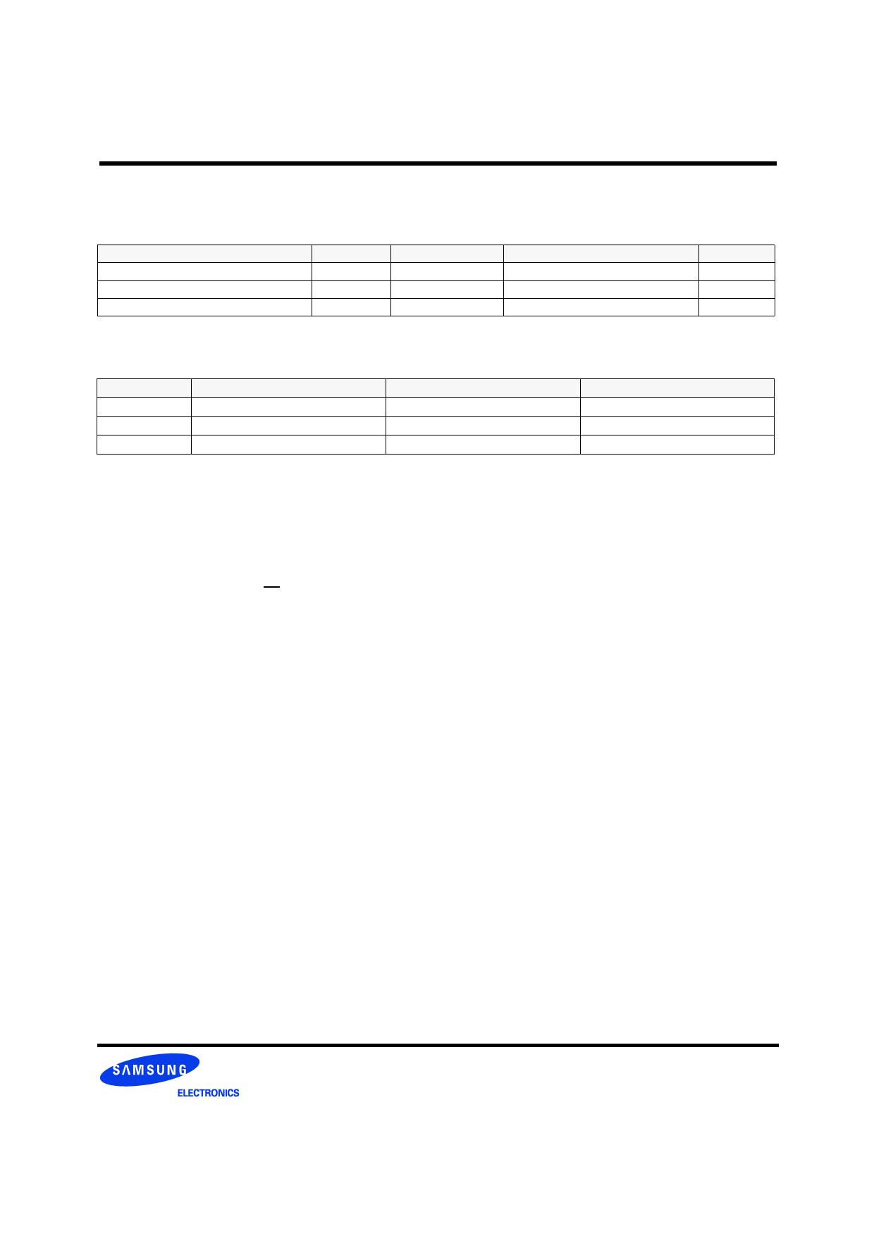
Ordering Information
Part Number
M312L2923BG0-CB3/A2/B0
M312L2920BG0-CB3/A2/B0
M312L5720BG0-CB3/A2/B0
Density
1GB
1GB
2GB
Organization
128M x 72
128M x 72
256M x 72
Component Composition
64Mx8( K4H510838B) * 18EA
128Mx4( K4H510438B) * 18EA
128Mx4( K4H510438B) * 36EA
Height
1,125mil
1,125mil
1,200mil
Operating Frequencies
Speed @CL2
Speed @CL2.5
CL-tRCD-tRP
B3(DDR333@CL=2.5)
133MHz
166MHz
2.5-3-3
A2(DDR266@CL=2)
133MHz
133MHz
2-3-3
B0(DDR266@CL=2.5)
100MHz
133MHz
2.5-3-3
Feature
• Power supply : Vdd: 2.5V ± 0.2V, Vddq: 2.5V ± 0.2V
• Double-data-rate architecture; two data transfers per clock cycle
• Bidirectional data strobe(DQS)
• Differential clock inputs(CK and CK)
• DLL aligns DQ and DQS transition with CK transition
• Programmable Read latency 2, 2.5 (clock)
• Programmable Burst length (2, 4, 8)
• Programmable Burst type (sequential & interleave)
• Edge aligned data output, center aligned data input
• Auto & Self refresh, 7.8us refresh interval(8K/64ms refresh)
• Serial presence detect with EEPROM
SAMSUNG ELECTRONICS CO., Ltd. reserves the right to change products and specifications without notice.
Rev. 1.1 August. 2003
Share Link: 