HSP45116AVC-52Z データシートの表示(PDF) - Intersil
部品番号
コンポーネント説明
一致するリスト
HSP45116AVC-52Z Datasheet PDF : 19 Pages
| |||
HSP45116A
Pin Descriptions
NAME
NUMBER
TYPE
DESCRIPTION
VCC
GND
22, 34, 50, 87, 95,
102, 111, 124, 132,
145, 159
7, 20, 32, 48, 62, 73,
83, 92, 98, 108,
114, 119, 125, 131,
143, 157
- +5V Power supply input.
- Power supply ground input.
C0-15
54-61, 63-70
I Control input bus for loading phase and frequency data into the PFCS. C15 is the MSB.
AD0-1
51, 52
I Address pins for selecting destination of C0-15 data. AD1 is the MSB.
CS
47
I Chip select (active low).
WR
53
I Write Enable. Data is clocked into the input register selected by AD0-1 on the rising edge of WR
when the CS line is low.
CLK
49
ENPHREG
27
I Clock. All registers, except the Control Registers clocked with WR, are clocked (when enabled)
by the rising edge of CLK.
I Phase Register Enable (active low). Registered on chip by CLK. When active low, after being
clocked onto chip, ENPHREG enables the clocking of data into the Phase Register.
ENOFREG
28
I Frequency Offset Register Enable (active low). Registered on chip by CLK. When active, after
being clocked onto chip, ENOFREG enables clocking of frequency offset data into the frequency
offset register.
ENCFREG
42
I Center Frequency Register Enable (active low). Registered on chip by CLK. When active, after
being clocked onto chip, ENCFREG enables clocking of data into the Center Frequency Register.
ENPHAC
43
ENTIREG
44
I Phase Accumulator Register Enable (active low). Registered on chip by CLK. When active, after
being clocked onto chip, ENPHAC enables clocking of the Phase Accumulator Register.
I Time Interval Control Register Enable (active low). Registered on chip by CLK. When active, after
being clocked onto chip, ENTIREG enables clocking of data into the Time Accumulator Register.
ENI
45
MODPI/2PI
46
I Real and Imaginary Data Input Register (RIR, IIR) Enable (active low). Registered on chip by
CLK. When active, after being clocked onto chip, ENI enables clocking of data into the real and
imaginary input data register.
I Modulo π/2π Select. When low, the Sine and Cosine ROMs are addressed modulo 2π (360
degrees). When high, the most significant address bit is held low so that the ROMs are addressed
modulo π (180 degrees). This input is registered on chip by clock. This control pin was included
for FFT processing.
CLROFR
41
LOAD
38
I Frequency Offset Register Output Zero (active low). Registered on chip by CLK. When active,
after being clocked onto chip, CLROFR zeros the data path from the Frequency Offset Register
to the frequency adder. New data can still be clocked into the Frequency Offset Register;
CLROFR does not affect the contents of the register.
I Phase Accumulator Load Control (active low). Registered on chip by CLK. Zeroes feedback path
in the phase accumulator without clearing the Phase Accumulator Register.
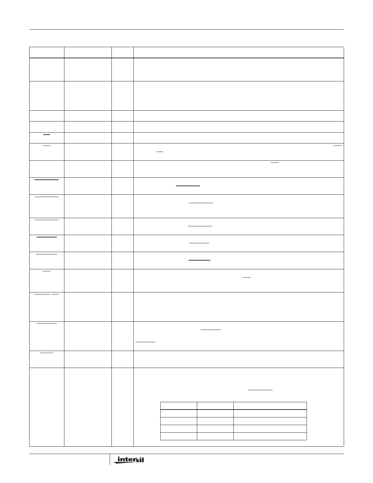
MOD0-1
35, 36
I External Modulation Control Bits. When selected with the PMSEL line, these bits add a 0, 90, 180,
or 270 degree offset to the current phase in the phase accumulator. The lower 14 bits of the phase
control path are set to zero.
These bits are loaded into the Phase Register when ENPHREG is low.
MOD1
0
0
1
1
MOD0
0
1
0
1
PHASE SHIFT (DEGREES)
0
90
270
180
4
FN4156.4
May 7, 2007
Share Link: 