HSP45116AVC-52Z データシートの表示(PDF) - Intersil
部品番号
コンポーネント説明
一致するリスト
HSP45116AVC-52Z Datasheet PDF : 19 Pages
| |||
HSP45116A
through 15 of the NCOM, with the output multiplexers set to
bring out the most significant bits of the CMAC output
(OUTMUX = 00). The most significant 16 bits out of the
PFCS appears on IOUT0-15 and the least significant bits
come out on ROUT0-15.
Complex Multiplier/Accumulator
The CMAC (Figure 1) performs two types of functions:
complex multiplication/accumulation for modulation and
demodulation of digital signals, and the operations
necessary to implement an FFT butterfly. Modulation and
demodulation are implemented using the complex multiplier
and its associated accumulator; the rest of the circuitry
in this section, i.e., the complex accumulator, input shifters
and growth detect logic are used along with the complex
multiplier/accumulator for FFTs. The complex multiplier
performs the complex vector multiplication on the output of
the Sine/Cosine Section and the vector represented by the
real and imaginary inputs RIN and IIN. The two vectors are
combined in the following manner:
ROUT = COS x RIN - SIN x IIN
IOUT = COS x IIN + SIN x RIN
RIN and IIN are latched into the Input Registers and passed
through the shift stages. Clocking of the Input Registers is
enabled with a low on ENI. The amount of shift on the
latched data is programmed with SH0-1 (Table 3). The
output of the shifters is sent to the CMAC and the auxiliary
accumulators.
TABLE 3. INPUT SHIFT SELECTION
SH1
SH0
SELECTED BITS
0
0
RIN0-15, IMIN0-15
0
1
RIN1-16, IMIN1-16
1
0
RIN2-17, IMIN2-17
1
1
RIN3-18, IMIN3-18
The 33-bit real and imaginary outputs of the Complex
Multiplier are latched in the Multiplier Registers and then go
through the Accumulator Section of the CMAC. If the ACC
line is high, the feedback to the accumulators is enabled; a
low on ACC zeroes the feedback path, so that the next set of
real and imaginary data out of the complex multiplier is
stored in the CMAC Output Registers.
The data in the CMAC Output Registers goes to the
Multiplexer, the output of which is determined by the
OUTMUX0- 1 lines (Table 4). BINFMT controls whether the
output of the Multiplexer is presented in two’s complement or
unsigned format; BINFMT = 0 inverts ROUT19 and IOUT19
for unsigned output, while BINFMT = 1 selects two’s
complement.
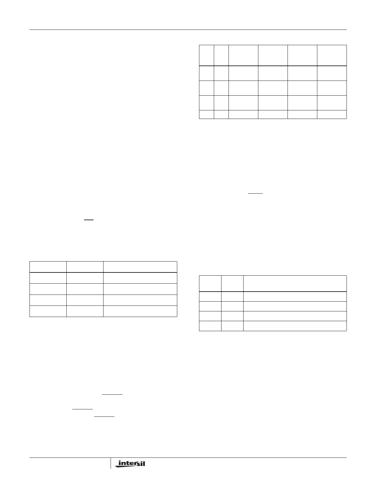
TABLE 4. OUTPUT MULTIPLEXER SELECTION
OUT OUT
MUX MUX
10
RO16-19
RO0-15
IO16-19
IO0-15
0 0 Real CMAC Real CMAC Imag CMAC Imag CMAC
31-34
15-30
31-34
15-30
0 1 Real CMAC 0, Real
Imag CMAC 0, Imag
31-34
CMAC 0-14 31-34
CMAC 0-14
1 0 Real ACC Real ACC Imag ACC Imag ACC
16-19
0-15
16-19
0-15
1 1 Reserved Reserved Reserved Reserved
The Complex Accumulator duplicates the accumulator in the
CMAC. The input comes from the data shifters, and its 20-bit
complex output goes to the Multiplexer. ACC controls
whether the accumulator is enabled or not. OUTMUX0-1
determines whether the accumulator output appears on
ROUT and IOUT.
The Growth Detect circuitry outputs a two bit value that
signifies the amount of growth on the data in the CMAC and
Complex Accumulator. Its output, DET0-1, is encoded as
shown in Table 5. If PEAK is low, the highest value of
DET0-1 is latched in the Growth Detect Output Register.
The relative weighting of the bits at the inputs and outputs of
the CMAC is shown in Figure 3. Note that the binary point of
the sine, cosine, RIN and IIN is to the right of the most
significant bit, while the binary point of RO and IO is to the
right of the fifth most significant bit. These CMAC external
input and output busses are aligned with each other to
facilitate cascading NCOMs for FFT applications.
TABLE 5. GROWTH ENCODING
DET 1 DET 0
NUMBER OF BITS
OF GROWTH ABOVE 2o
0
0
0
0
1
1
1
0
2
1
1
3
11
FN4156.4
May 7, 2007
Share Link: 