AS1324 データシートの表示(PDF) - austriamicrosystems AG
部品番号
コンポーネント説明
一致するリスト
AS1324 Datasheet PDF : 21 Pages
| |||
AS1324
Datasheet - Application Information
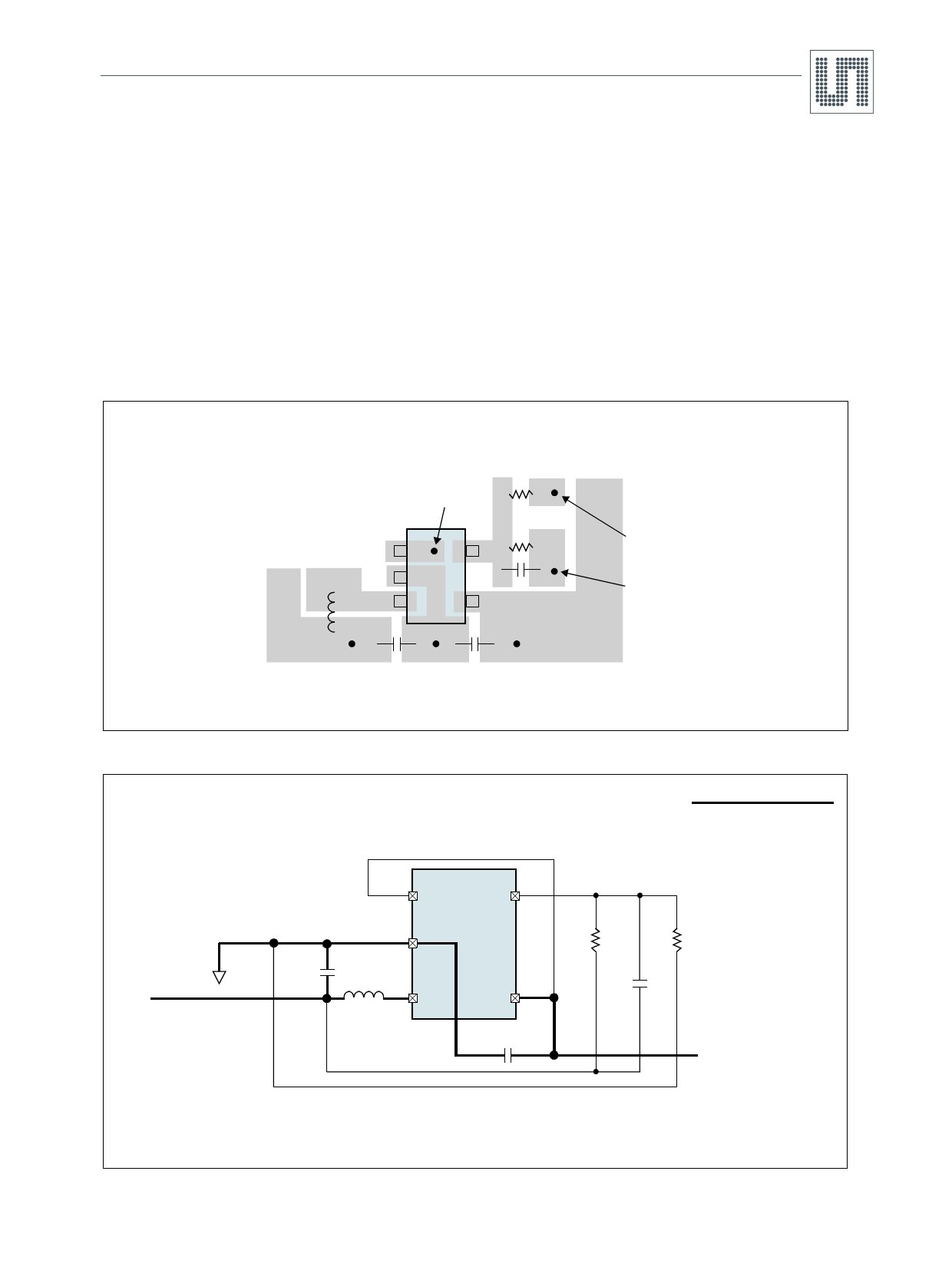
9.10 Layout Considerations
The AS1324 requires proper layout and design techniques for optimum performance.
The power traces (GND, SW, and VIN) should be kept as short, direct, and wide as is practical.
Pin VFB (AS1324 only) should be connected directly to the feedback resistors (R1 and R2). A potentiometer as replacement for R1 and R2
should be avoided to minimize the output voltage ripple and to maintain the stability of the regulator.
The resistive divider (R1/R2) must be connected between the positive plate of COUT and ground.
The positive plate of CIN should be connected as close to VIN as is practical since CIN provides the AC current to the internal power MOS-
FETs.
Switching node SW should be kept far away from the sensitive VFB node.
The negative plates of CIN and COUT should be kept as close to each other as is practical. A starpoint to Ground is recommended.
Figure 29. AS1324 Basic PCB Layout
VOUT
R1
Via to VIN
1
5
L1
2 AS1324
SW 3
4
R2
CFWD
COUT
CIN
GND
VIN
Via to GND
Via to VOUT
Figure 30. AS1324 Basic Diagram
High Current Path
VOUT
1
EN
2
GND
COUT
3
L1 SW
5
VFB
AS1324
4
VIN
CIN
R2
CFWD
R1
VIN
www.ams.com/DC-DC_Step-Up/AS1324
Revision 1.06
16 - 21
Share Link: 