MAX9546 データシートの表示(PDF) - Maxim Integrated
部品番号
コンポーネント説明
一致するリスト
MAX9546 Datasheet PDF : 17 Pages
| |||
MAX9546/MAX9547
Differential Video Interface Chipset
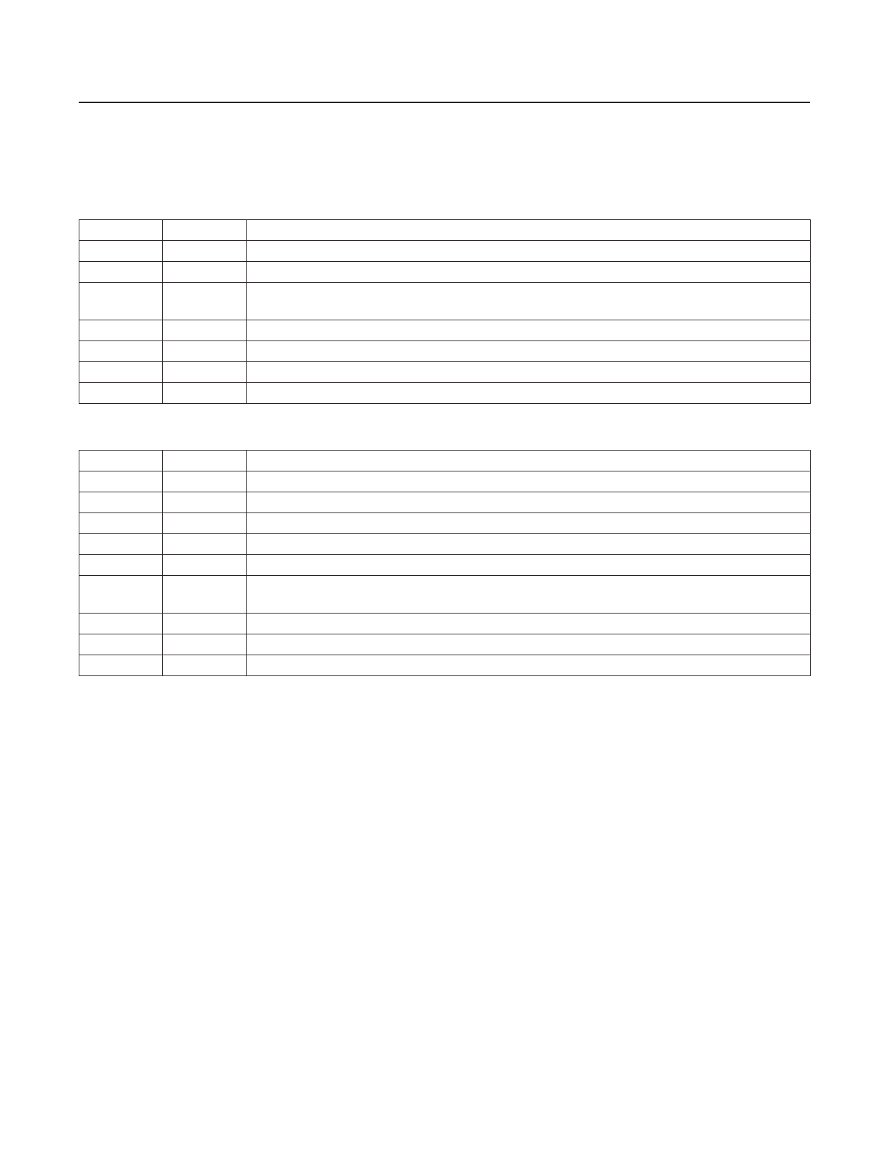
Pin Description (MAX9546)
PIN
NAME
FUNCTION
1, 8
VCC
Power Supply. Connect together and bypass with a 0.1µF in parallel with a 4.7µF capacitor to GND.
2
IN
Video Input
3
FAULT
Fault Indicator. Active-low, open-drain output. FAULT = low when fault is detected at the output.
FAULT = high when no fault is detected at the output.
4, 5
GND
Ground
6
OUT- Negative Differential Output
7
OUT+ Positive Differential Output
EP
EP
Exposed Paddle. Connect to GND.
Pin Description (MAX9547)
PIN
NAME
FUNCTION
1
IN+
Positive Differential Input
2
ZT+
Positive Transconductance Terminal
3
ZT-
Negative Transconductance Terminal
4
IN-
Negative Differential Input
5
GND
Ground
6
LOS
Loss-of-Signal Indicator. Active-low, open-drain output. LOS = low when no signal is detected at the
input. LOS = high when signal is present at the input.
7
IOUT Current Output
8
VCC
Power Supply. Bypass with a 0.1µF capacitor in parallel with a 4.7µF capacitor to GND.
EP
EP
Exposed Paddle. Connect to GND.
Detailed Description
The MAX9546/MAX9547 differential interface chipset
converts single-ended voltages to differential voltages for
transport and then converts back to single-ended voltag-
es. The chipset is optimized for transporting CVBS/FBAS
analog video signals (PAL or NTSC) through hostile envi-
ronments. The MAX9546 driver includes a fault output
(FAULT) that indicates shorted transmission cables. The
MAX9547 receiver loss-of-signal output (LOS) indicates
an absence of input signal.
The MAX9546/MAX9547 operate from a 7.5V to 10V
single supply. The differential interface is immune to short-
circuit conditions to supply (VCC), or ground. These devic-
es include ±15kV ESD (Human Body Model) protection.
MAX9546
Driver
The MAX9546 driver converts a single-ended video input
into a differential output for transport across a twisted pair
of wires. The input is AC-coupled and the video signal
sync tip is clamped at 3.46V to set the voltage of the input.
The output common-mode voltage is optimized to reject
ground differences between the MAX9546 and MAX9547
up to ±2V. The differential gain is internally set to 2V/V to
drive a back-terminated output to unity gain. The maxi-
mum input resistance should not exceed 400Ω to ensure
device stability.
www.maximintegrated.com
Maxim Integrated │ 8
Share Link: 