HPMX-2003-T10 データシートの表示(PDF) - HP => Agilent Technologies
部品番号
コンポーネント説明
一致するリスト
HPMX-2003-T10 Datasheet PDF : 16 Pages
| |||
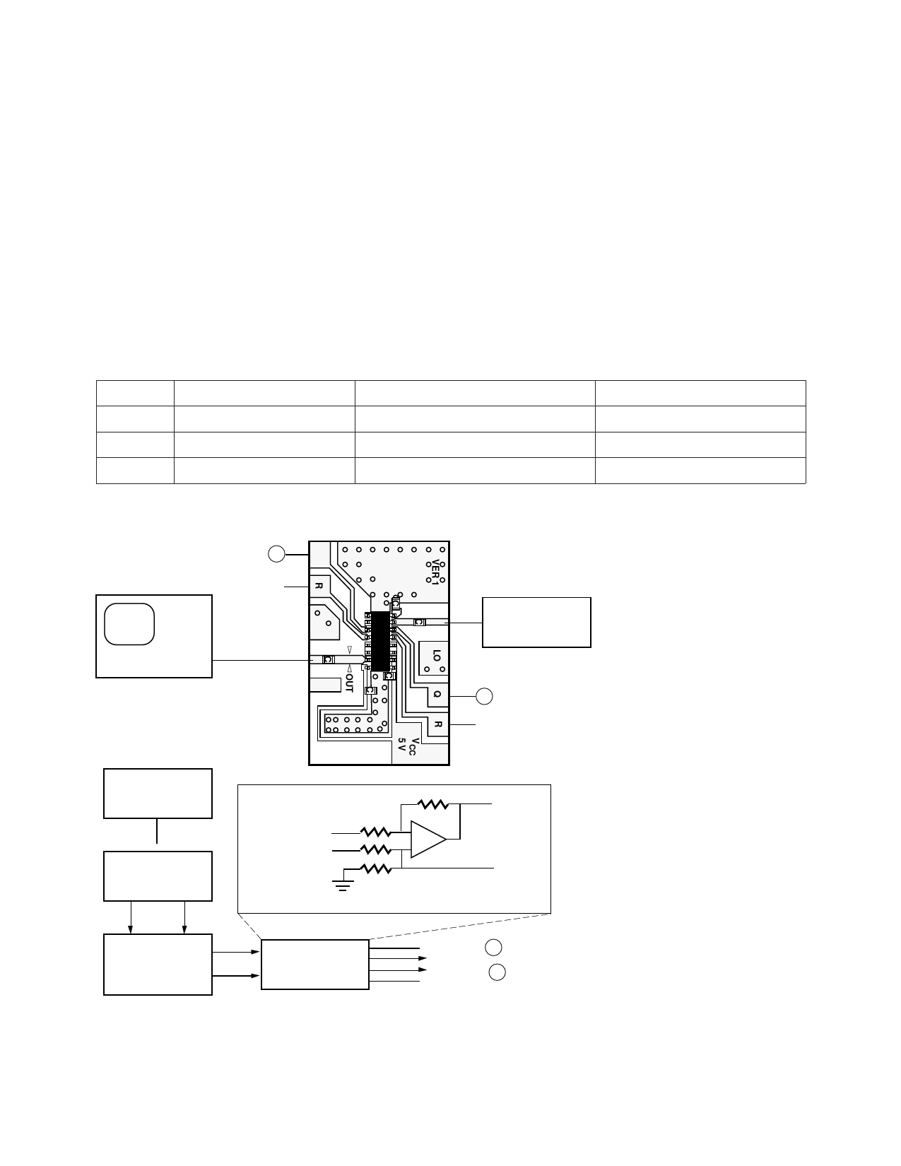
HPMX-2003 Modulation
Spectrum Diagrams
Figure 20, below, shows the test
setup that was used to generate
the modulation spectrum dia-
grams that appear on the GSM,
JDC and NADC applications pages
of this data sheet. The major dif-
ferences between the tests are
summarized in the table below.
The modulation spectra are cre-
ated by setting the function gen-
erator to the appropriate bit-clock
frequency. The pattern generator
is set to produce a pseudorandom
serial bit stream (n␣ = 20) that is
NRZ coded. The pseudorandom
bit stream which simulates the
serial data in a digital phone is fed
to the base-band processor that
splits it into a two bit parallel
stream (I and Q) and then filters
each according to the require-
ments of the digital telephone sys-
tem being simulated. The I and Q
signals from the baseband filter
are then DC offset by 2.5 V using
the op-amp circuit. The output of
the modulator is monitored using
a spectrum analyzer.
System
GSM
JDC
NADC
Bit Clock Frequency
270 kHz
42 kHz
48.6 kHz
Baseband Filter
0.3 GMSK (HP 8657B)
α = 0.5 π/4 DQPSK (HP 8657D)
α = 0.35 π/4 DQPSK (HP 8657D)
Channel (LO) Frequency
900 MHz
950 MHz
835 MHz
1
Iref
HP-8563E
SPECTRUM ANALYZER
HPMX-2003/5
H
HP-8657B
SIGNAL GENERATOR
835-950 MHz
2
Qref
HP-3314A
FUNCTION
GENERATOR
HP-3780A
PRBS GENERATOR
CLOCK
DATA
π/4DQPSK Q INPUT
+5 V
•–
•+
Q + 2.5 V
Qref = 2.5 V
ALL R = 5 k
OP-AMP: TL-084
I CHANNEL IS IDENTICAL
HP-8657B
OR
HP-8657D
BASEBAND
PROCESSOR
I
OP-AMP CIRCUIT
Q
(SEE ABOVE)
I + 2.5 V TO 1
2.5 V TO Iref
Q + 2.5 V TO 2
2.5 V TO Qref
Figure 20. Test Equipment Setup for Modulation Spectrum Diagrams.
7-46
Share Link: 