HPMX-2003-T10 データシートの表示(PDF) - HP => Agilent Technologies
部品番号
コンポーネント説明
一致するリスト
HPMX-2003-T10 Datasheet PDF : 16 Pages
| |||
HPMX-2003 GSM
Applications
The GSM System
GSM (Group Speciale Mobile)
commonly refers to the European
digital cellular telephone system
standard. Digital cellular phones
for the European market must
conform to this standard. The
GSM system is characterized by
200 kHz channel spacing and mo-
bile to base transmit frequencies
of 890 - 915 MHz. The primary
modulation characteristics in-
clude 0.3 GMSK filtering of the I
and Q signals and 270 kbps trans-
mission rate.
Critical Performance
Parameters
GSM standards require that the
telephone exhibit RMS phase er-
ror ≤ 5°and peak phase error <20°.
The modulated output spectrum
of the phone must lie within a
“spectral mask” which defines
maximum allowable radiation lev-
els into adjacent and alternate
channels. Specifically, 200 kHz
from the channel center frequency
(f0), the output of the phone must
be at least 30 dB below the peak
output at f0. 400 kHz from f0 the
output must be 50-60 dB below
the peak output at f0 depending
upon the class of radio. Refer to
the GSM900 specifi-cations for
more detailed information.
HPMX-2003 Performance
Typical RMS phase error level of
2° and typical peak levels of 8°
makes the HPMX-2003 an excel-
lent choice for GSM applications.
The output spectrum falls easily
within the GSM spectral mask,
and the high power and simple
output configuration mean lower
components count, reduced size
and higher system efficiency.
Particulars of Use
Many of the GSM application
performance graphs shown in this
data sheet were created using the
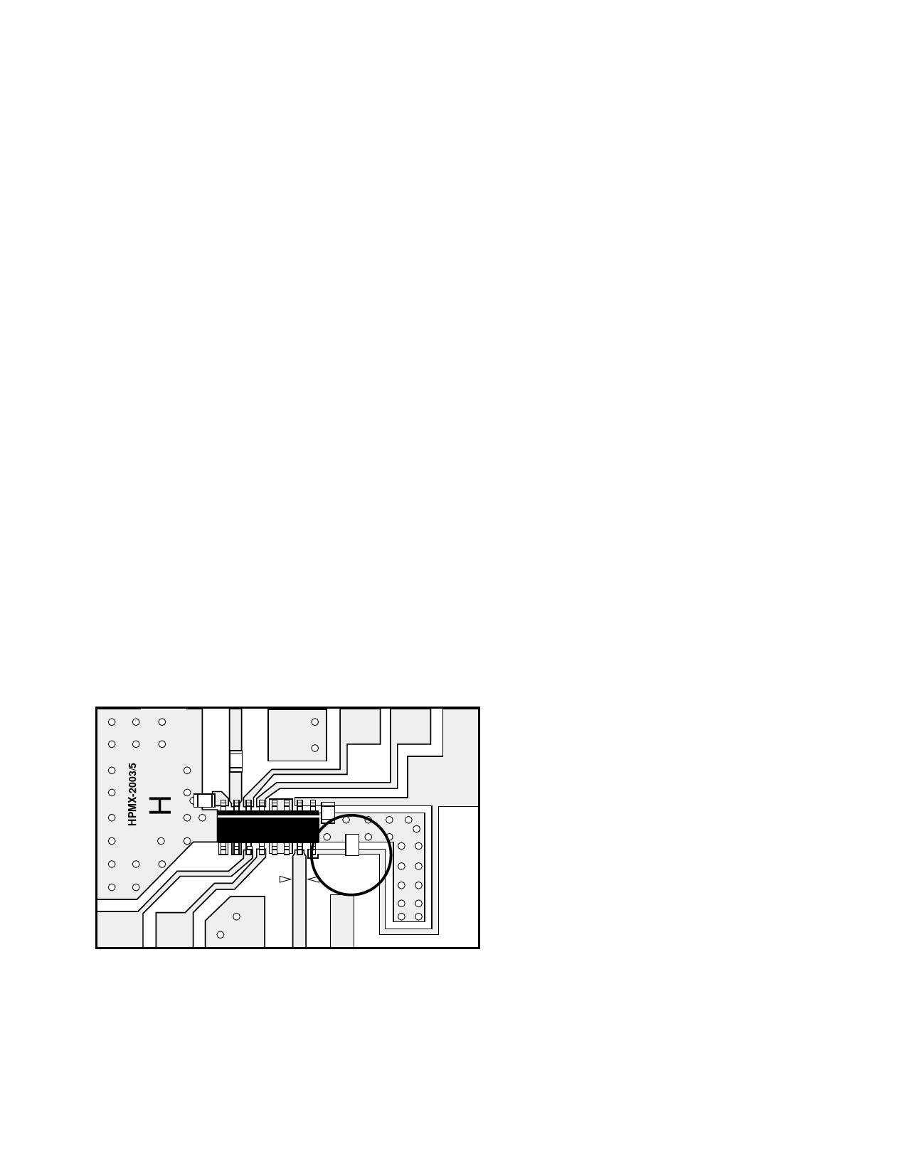
test board shown in figure 21,
below.
The only external components re-
quired by this IC are four chip
capacitors. One capacitor is used
as a DC block on the input trans-
mission line. The second capaci-
tor (at pin 8) provides an AC
ground to one side of the differen-
tial LO input. The third and fourth
capacitors (at pins 1 and 16) are
for VCC bypass.
The circuit board includes an in-
ductive trace that can optionally
be used to minimize output VSWR
by placing a bypass capacitor at
various points along the inductive
line. Minimum VSWR for GSM
applications is achieved by plac-
ing the capacitor as shown in the
circle (inductance ≈2 nH).
The IC has an internal blocking
capacitor so the output is a simple
50 Ω transmission line. An
enlarged scale layout of the test
board can be found on the last
page of this data sheet.
VER. 1
C
C
LO
Q
C
C
OUT
R
VCC
5V
I
R
Figure 21. HPMX-2003 GSM Test Board.
7-47
Share Link: 