HPMX-2003-T10 データシートの表示(PDF) - HP => Agilent Technologies
部品番号
コンポーネント説明
一致するリスト
HPMX-2003-T10 Datasheet PDF : 16 Pages
| |||
HPMX-2003 Pin
Description
VCC (pins 1,2)
These two pins provide DC power
to the mixers in the RFIC, and are
connected together internal to the
package. They should be con-
nected to a 5 V supply, with appro-
priate AC bypassing (1000 pF typ.)
used near the pins, as shown in
figures 1 and 2. The voltage on
these pins should always be
kept at least 0.8 V more posi-
tive than the DC level on any
of pins 5, 6, 11, or 12. Failure to
do so may result in the modulator
drawing sufficient current
through the data or reference
inputs to damage the IC.
Ground (pins 3, 4, 10, 13 & 14)
These pins should connect with
minimal inductance to a solid
ground plane (usually the back-
side of the PC board). Recom-
mended assembly employs
multiple plated through via holes
where these leads contact the PC
board.
Iref (pin 12) and Q ref (pin 5),
I␣ (pin 11) and Q (pin 6) Inputs
The I and Q inputs are designed
for unbalanced operation but can
be driven differentially with simi-
lar performance. The recom-
mended level of unbalanced I and
Q signals is 2.5 Vp-p with an aver-
age level of 2.5 V above ground.
The reference pins should be DC
biased to this average data signal
level (VCC/2 or 2.5 V typ.). For
single ended drive, pins 5 and 12
can be tied together. For balanced
operation, 2.5 Vp-p signals may be
applied across the Imod/Iref and the
Qmod/Qref pairs. The average level
of all four signals should be about
2.5 V above ground. The imped-
ance between any I or Q and
ground is typically 10 K Ω and the
impedance between Imod and Iref or
Qmod and Qref is typically 10 KΩ.
The input bandwidth typically
exceeds 40 MHz. It is possible to
reduce LO leakage through the IC
by applying slight DC imbalances
between Imod and Iref and/or Qmod
and Qref (see section entitled
“HPMX-2003 Using Offsets to Im-
prove Lo Leakage”). All perfor-
mance data shown on this data
sheet was taken with unbalanced
I/Q inputs.
LO Input (pins 7 and 8)
The LO input of the HPMX-2003 is
balanced and matched to 50 For
drive from an unbalanced LO, pin
7 should be AC coupled to the LO
using a 50 Ω transmission line and
a blocking capacitor (1000 pF
typ.), and pin 8 should be AC
grounded (1000 pF capacitor
typ.), as shown in figure 1. For
drive from a balanced LO source,
50 Ω transmission lines and block-
ing capacitors (1000 pF typ.) are
used on both pins 7 and 8, as
shown in figure 2. The internal
phase shifter allows operation
from 800 - 1000 MHz. The recom-
mended LO input level is -12 dBm.
All performance data shown on
this data sheet was taken with un-
balanced LO operation.
RF Output (pin15)
The RF output of the HPMX-2003
is configured for unbalanced
operation. The output is internally
DC blocked and matched to 50 Ω,
so a simple 50 Ω microstrip line is
all that is required to connect the
modulator to other circuits.
VCCL (pin 16)
Pin 16 is the VCC input for the out-
put stage of the IC. It is not inter-
nally connected to the other VCC
pins. The external connection al-
lows the addition of a small induc-
tor (0 - 6 nH) to tune the output
for minimum VSWR, depending
upon the operating frequency.
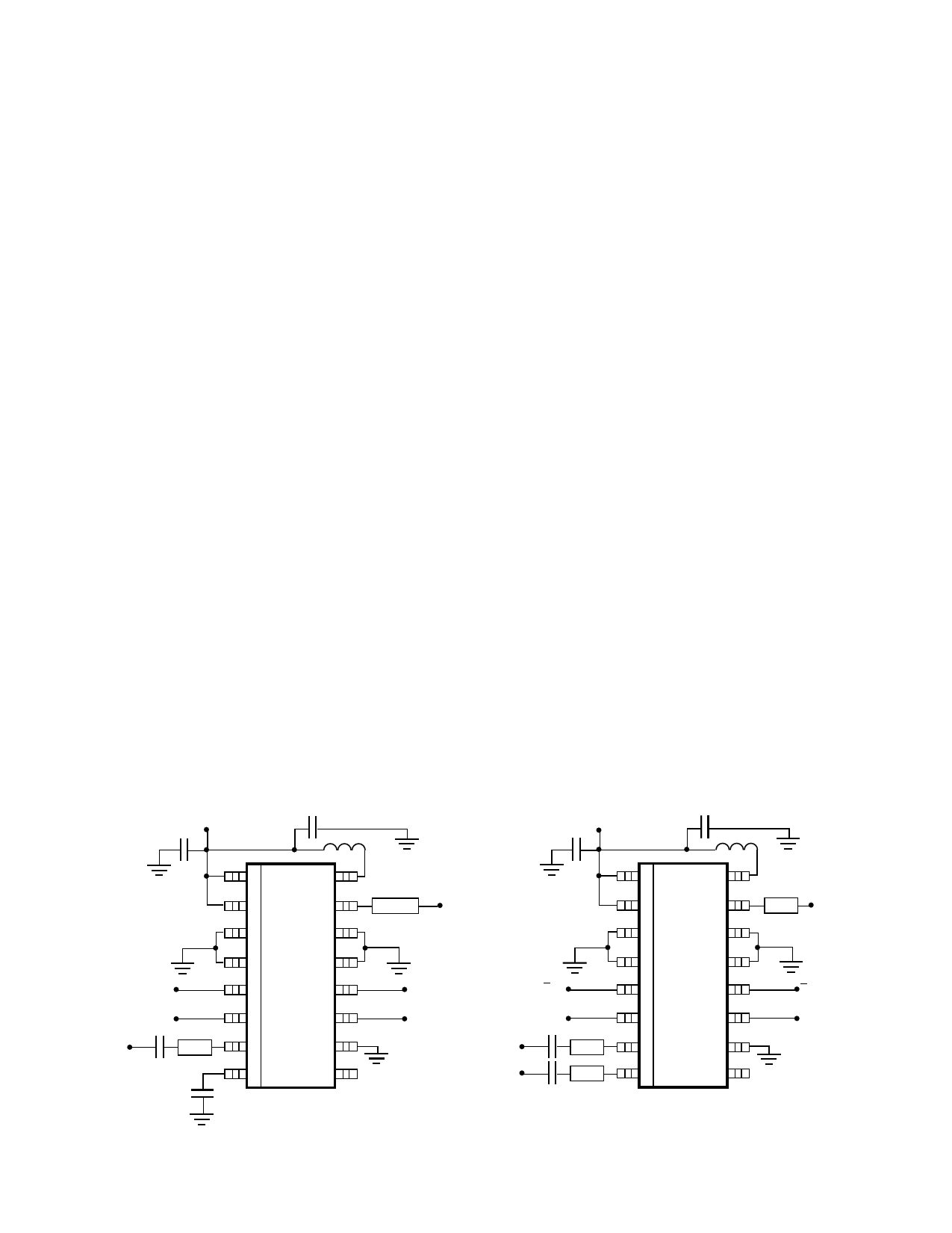
+5 V
1000 pF
Qref
Qmod
LOin
1000 pF
1000 pF
1000 pF
+5 V
1000 pF
OPTIONAL INDUCTOR
1
16
2
15
3
14
RFout
4
13
5
12
Iref
Qref
6
11
7
10
Imod
LOin+
Qmod
1000 pF
8
9
DO NOT CONNECT
LOin–
1000 pF
1000 pF
OPTIONAL INDUCTOR
1
16
2
15
3
14
RFout
4
13
5
12
6
11
I ref
Imod
7
10
8
9
DO NOT CONNECT
Figure 1. HPMX-2003 Connections Showing Unbalanced LO
and I, Q Inputs.
Figure 2. HPMX-2003 Connections Showing Balanced LO
and I, Q Inputs.
7-40
Share Link: 