DS21448 データシートの表示(PDF) - Maxim Integrated
部品番号
コンポーネント説明
一致するリスト
DS21448 Datasheet PDF : 60 Pages
| |||
DS21448 3.3V T1/E1/J1 Quad Line Interface
4.3 Parallel Port Operation
The option for either multiplexed bus operation (BIS0 = 0) or nonmultiplexed bus operation (BIS0 = 1) is available
when using the parallel interface. The DS21448 can operate with either Intel or Motorola bus timing configurations.
If the PBTS pin is wired low, Intel timing is selected; if wired high, Motorola timing is selected. All Motorola bus
signals are listed in parentheses (). Four sets of identical register maps exist, one for each channel. See Table 4-H
for register names and addresses. Use the appropriate chip select (CS1, CS2, CS3, or CS4) to access a channel’s
register map. See the timing diagrams in Section 10 for more details. Hardware and serial port modes are not
supported when using parallel port operation.
4.3.1 Device Power-Up and Reset
The DS21448 resets itself upon power-up, setting all writeable registers to 00h and clearing the status and
information registers. CCR3.7 (TUA1) = 0 results in the LIU transmitting unframed all ones. After the power
supplies have settled, initialize all control registers to the desired settings, then toggle the LIRST bit (CCR3.2). The
DS21448 can at any time be reset to the default settings by bringing HRST low (level triggered) or by powering
down and powering up again.
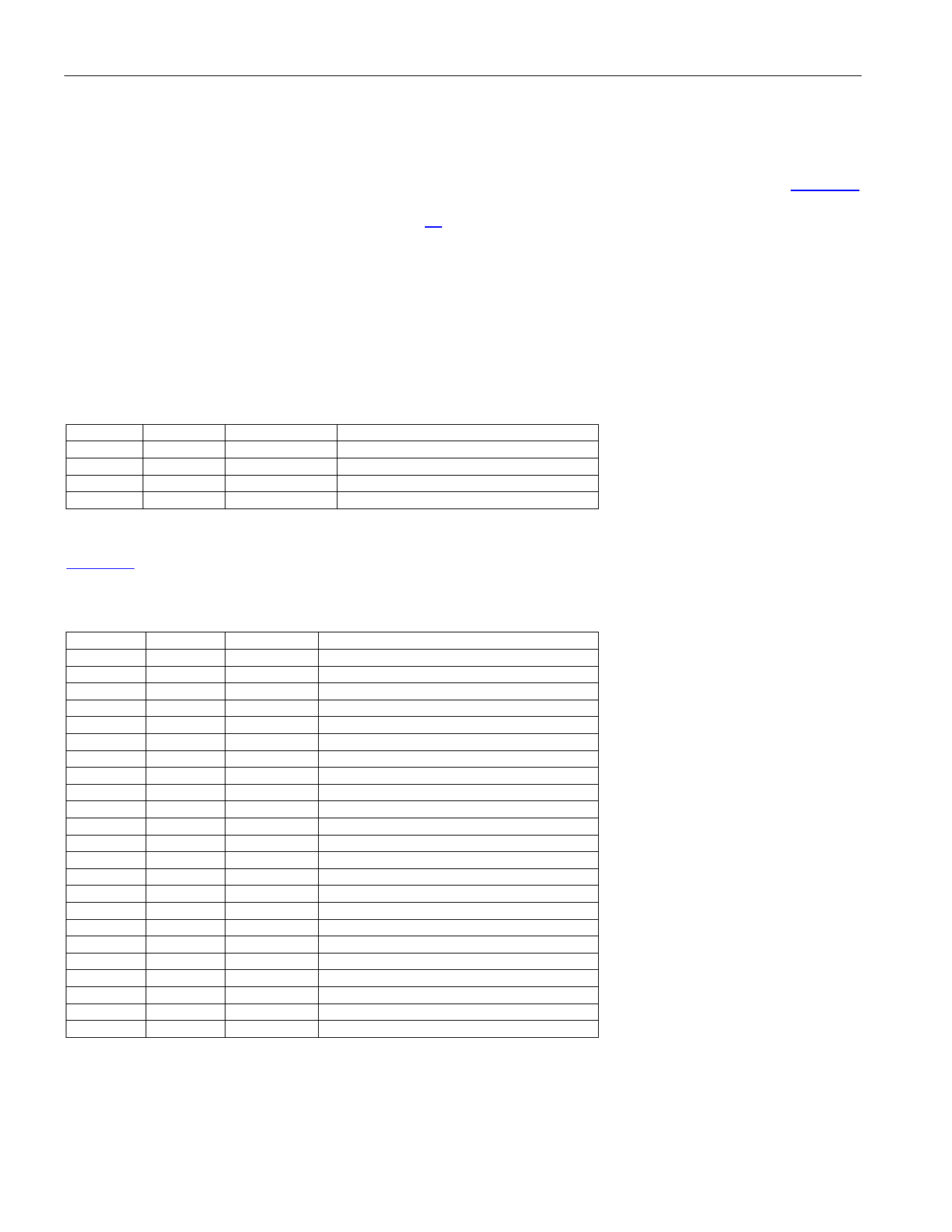
Table 4-G. Parallel Port Mode Selection
PBTS
0
0
1
1
BIS0
0
1
0
1
PROCESSOR
Intel
Intel
Motorola
Motorola
BUS INTERFACE TYPE
Parallel Port Mode (Multiplexed)
Parallel Port Mode (Nonmultiplexed)
Parallel Port Mode (Multiplexed)
Parallel Port Mode (Nonmultiplexed)
4.3.2 Register Map
Table 4-H shows the typical register map for all four ports. Use the appropriate chip select (CS1, CS2, CS3, or CS4)
to access a channel’s register map.
Table 4-H. Register Map
NAME
R/W
ADDRESS
CCR1
R/W
00h
CCR2
R/W
01h
CCR3
R/W
02h
CCR4
R/W
03h
CCR5
R/W
04h
CCR6
R/W
05h
SR
R
06h
IMR
R/W
07h
RIR1
R
08h
RIR2
R
09h
IBCC
R/W
0Ah
TCD1
R/W
0Bh
TCD2
R/W
0Ch
RUPCD1
R/W
0Dh
RUPCD2
R/W
0Eh
RDNCD1
R/W
0Fh
RDNCD2
R/W
10h
ECR1
R
11h
ECR2
R
12h
TEST1
R/W
13h
TEST2
R/W
14h
TEST2
R/W
15h
—
—
(Note 1)
FUNCTION
Common Control Register 1
Common Control Register 2
Common Control Register 3
Common Control Register 4
Common Control Register 5
Common Control Register 6
Status Register
Interrupt Mask Register
Receive Information Register 1
Receive Information Register 2
In-Band Code Control Register
Transmit Code Definition Register 1
Transmit Code Definition Register 2
Receive-Up Code Definition Register 1
Receive-Up Code Definition Register 2
Receive-Down Code Definition Register 1
Receive-Down Code Definition Register 2
Error Count Register 1
Error Count Register 2
Test 1
Test 2
Test 3
—
Note 1: Register addresses 16h–1Fh do not exist.
18 of 60
Share Link: 