DS21448 データシートの表示(PDF) - Maxim Integrated
部品番号
コンポーネント説明
一致するリスト
DS21448 Datasheet PDF : 60 Pages
| |||
DS21448 3.3V T1/E1/J1 Quad Line Interface
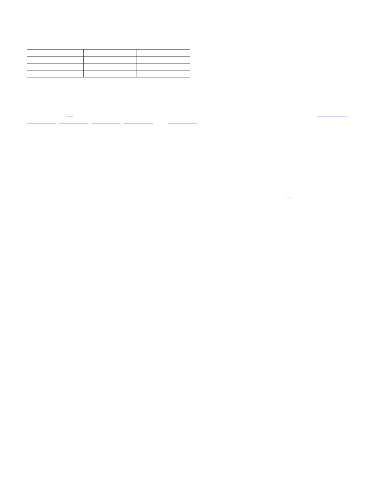
Table 4-F. MCLK Selection in Hardware Mode
MCLK (MHz)
JAMUX
ETS
2.048
0
0
2.048
1
1
1.544
0
1
4.2 Serial Port Operation
Setting BIS1 = 1 and BIS0 = 0 enables the serial bus interface on the DS21448 (Table 2-A). Serial port read/write
timing is unrelated to the system transmit and receive timing, allowing asynchronous reads or writes by the host.
See Section 10 for the AC timing of the serial port. All serial port accesses are LSB first. See Figure 4-1,
Figure 4-2, Figure 4-3, Figure 4-4, Figure 4-5, and Figure 4-6 for additional details.
A serial bus access requires the use of four signals: serial clock (SCLK), one of the four chip selects (CS), serial
data input (SDI), and serial data output (SDO). The DS21448 uses SCLK to sample data that is present on SDI and
output data onto SDO. Input clock-edge select (ICES) allows the user to choose which SCLK edge input data is
sampled on. Output clock-edge select (OCES) allows the user to choose which SCLK edge output data changes
on. When ICES is low, input data is latched on the rising edge of SCLK, and when ICES is high, input data is
latched on the falling edge of SCLK. When OCES is low, data is output on the falling edge of SCLK, and when
OCES is high, data is output on the rising edge of SCLK. Data is held until the next falling or rising edge of SCLK.
All data transfers are initiated by driving the appropriate port’s CS input low and ends with CS going inactive. CS
must go inactive between data transfers. See the serial bus timing information in Section 10 for details. All data
transfers are terminated if the port’s CS input transitions high. Port control logic is disabled, and SDO is tri-stated
when all CS pins are inactive.
Reading from or writing to the internal registers requires writing one address/command byte prior to the transferring
register data. Two types of serial bus transfers exist, standard and burst. The standard serial bus access always
consists of two bytes, an address/command byte that is always supplied by the user on SDI, and a data byte that
can either be written to the DS21448 using SDI (write operation) or output by the DS21448 on SDO (read
operation). The burst serial bus access consists of a single address/command byte followed either by 22 read or 22
write data bytes.
The first bit written (LSB) of the address/command byte specifies whether the access is to be a read (1) or a write
(0). The next 5 bits identify the register address. Valid register addresses are 00h through 15h. Bit 7 is reserved
and must be set to 0 for proper operation. Bit 8, the last bit (MSB) of the address/command byte, is the burst mode-
enable bit. When the burst bit is enabled (set to 0) and a READ operation is performed, the DS21448 automatically
outputs the contents of registers 00h through 15h sequentially, starting with register address 00h. When the burst
bit is enabled and a WRITE operation is performed, data supplied on SDI is sequentially written into the DS21448’s
register space starting at address 00h. Burst operation is stopped once address 15h is read or CS goes inactive.
For both burst read and burst write transfers, the address/command byte’s register address bits must be set to 0.
The user can broadcast register write accesses to multiple ports simultaneously by enabling the desired channels’
chip selects at the same time. However, only one port can be read at a time. Any attempt to read multiple ports
simultaneously results in invalid data being returned on SDO.
15 of 60
Share Link: 