MSM9405MB データシートの表示(PDF) - Oki Electric Industry
部品番号
コンポーネント説明
一致するリスト
MSM9405MB Datasheet PDF : 30 Pages
| |||
¡ Semiconductor
MSM9405
Time-out
The MSM9405 outputs an interrupt request or DMA request depending on the register setting
when the following time-out occurs even if the received data is below the receiving threshold
level:
The condition causing time-out in MIR or FIR mode is:
At least 1-byte data is in the receiving FIFO and 69.5 ms has passed after data is written from
the receiving shift register to the FIFO. During this period, the CPU or DMA controller does
not read the FIFO data.
The condition causing time-out in SIR or Extended SIR mode is:
At least 1-byte data is in the receiving FIFO and time (Tout) has passed after data is written
from the receiving shift register to the FIFO. During this period, the CPU or DMA controller
does not read the FIFO data.
Tout = 4 ¥ 8 ¥ 1/baud rate
baud rate: Transfer rate (2.4 to 115.2 kbps)
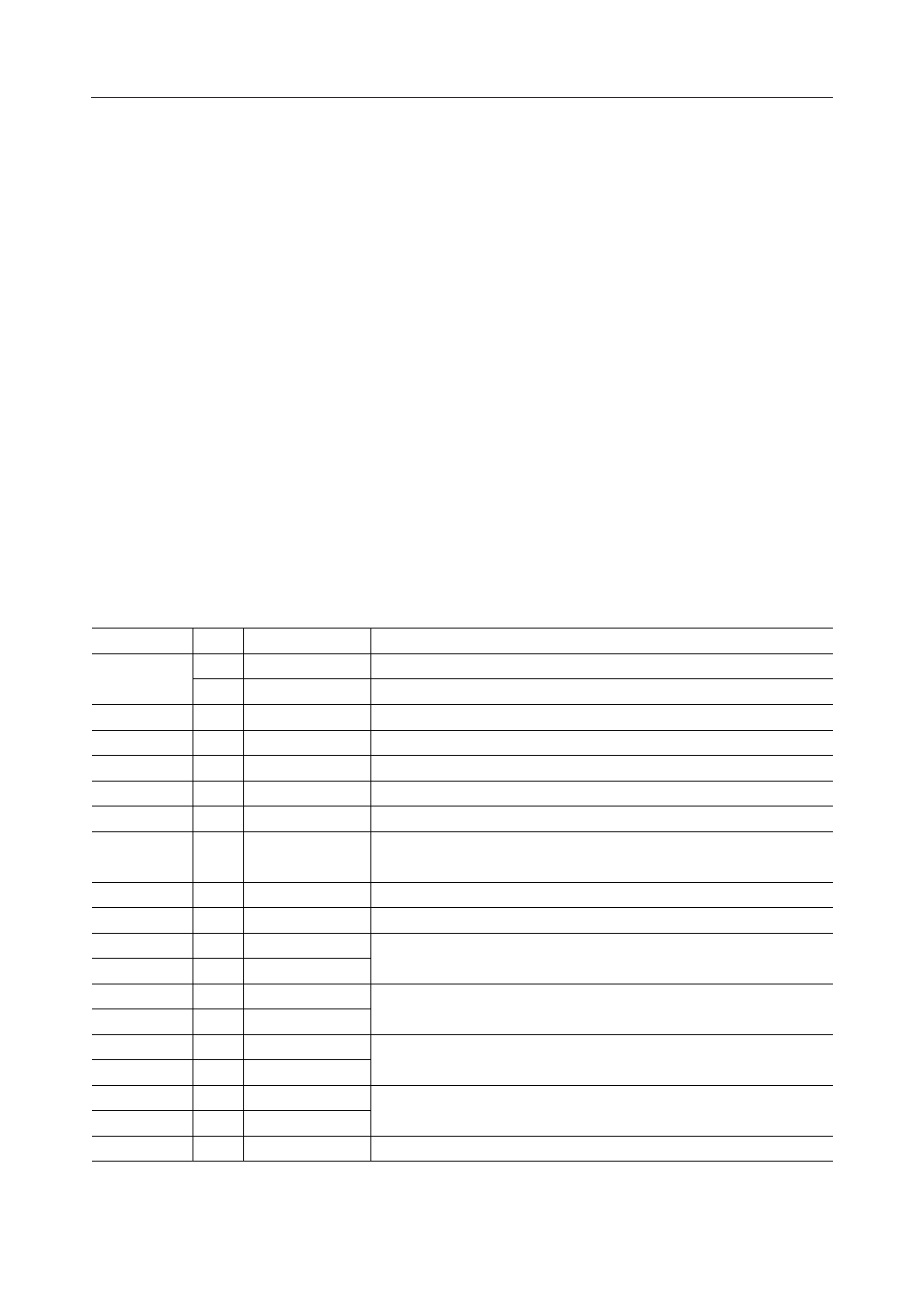
Register Map
The MSM9405 contains 14 registers, of which 13 are available. Each register can be selected with
the register address assigned from 0h through Ch. Various setting options are provided for each
register to allow optimum communication.
The registers are listed below. The register table is given on the next page.
A3-A0
0h
1h
2h
3h
4h
5h
6h
7h
8h
9h
Ah
9h
Ah
Bh
0h
Bh
Ch
Fh
R/W Register Name
R RDR
W TDR
R/W ENR
R EIR
R LSR
R/W ICR1
R/W ICR2
R/W MSR
R/W DSR
R/W FCR
R/W TFL (L)
*1
R/W TFL (H)
*1
R TCC (L)
*1
R TCC (H) *1
R/W MDS (L) *2
R/W MDS (H) *2
R RST (L) *2
R RST (H) *2
R/W TEST
Description
Receive data register
Transmit data register
Interrupt enable register
Interrupt event and status indication register
Status register
Transmit-receive control register
BOF count setting register
Register for setting a transfer mode and a data rate and selecting a
crystal to be used
DMA mode setting register
FIFO threshold setting register
Transmit frame-length setting register (low-order byte)
Transmit frame-length setting register (high-order byte)
Transmitter current-count register (low-order byte)
Transmitter current-count register (high-order byte)
Maximum data size setting register (low-order byte)
Maximum data size setting register (high-order byte)
Receiver frame length stack register (low-order byte)
Receiver frame length stack register (high-order byte)
Used for test.
*1 Whether TFL or TCC is read depends on the setting of the CTEST bit in the MSR
register.
*2 Whether MDS or RST is read depends on the setting of the CTEST bit in the MSR
register.
14/30
Share Link: 