10XSD200 データシートの表示(PDF) - Freescale Semiconductor
部品番号
コンポーネント説明
一致するリスト
10XSD200 Datasheet PDF : 60 Pages
| |||
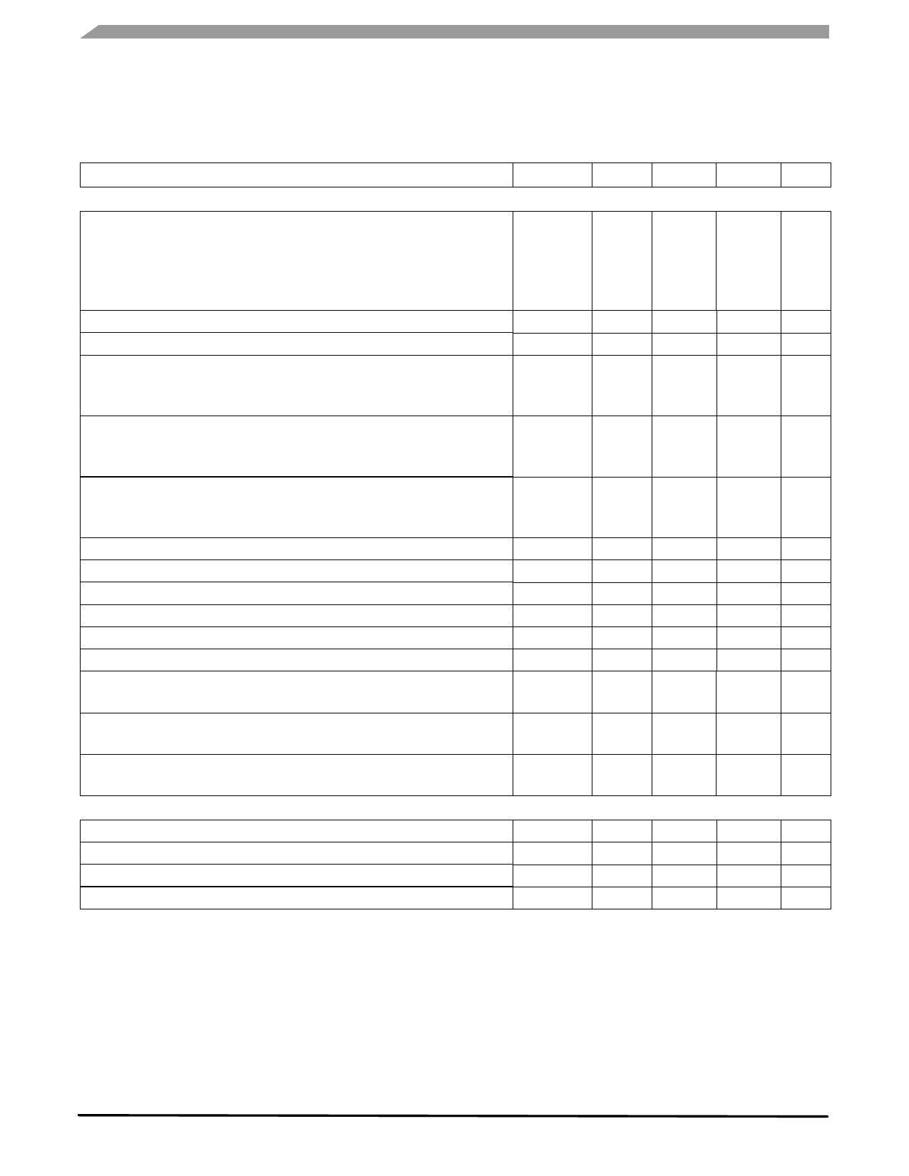
ELECTRICAL CHARACTERISTICS
DYNAMIC ELECTRICAL CHARACTERISTICS
Table 4. Dynamic Electrical Characteristics (continued)
Unless specified otherwise: 8.0 V VPWR 36 V, 3.0 V VDD 5.5 V, -40 C TA 125 C, GND = 0 V. Typical values are
average values evaluated under nominal conditions TA = 25 °C,VPWR = 28 V & VDD = 5.0 V, unless specified otherwise.
Parameter
Symbol
Min
Typ
Max
Unit
SWITCHING CHARACTERISTICS (CONTINUED)
Delay time difference from one channel to the other in parallel mode(30)
16 V < VPWR < 36 V
SR[1:0] = 00
SR[1:0] = 01
SR[1:0] = 10
Fault Detection Delay Time(31)
Output Shutdown Delay Time(32)
Current sense output settling Time for SR[1:0] = 00 (medium slew rate)
VPWR = 28 V (33)
16 V < VPWR < 36 V (34)
t(DLY)
s
-25
0.0
+25
-50
0.0
+50
-12
0.0
+12
tFAULT
–
tDETECT
–
5.0
8.0
s
7.0
12
s
t CSNSVAL_00
–
104
s
–
0.0
–
250
Current sense output settling Time for SR[1:0] = 01(low slew rate)
VPWR = 28 V (33)
16 V < VPWR < 36 V (34)
t CSNSVAL_01
–
167
s
–
0.0
–
355
Current sense output settling Time for SR[1:0] = 10 (high slew rate)
VPWR = 28 V (33)
16 V < VPWR < 36 V (34)
t CSNSVAL_10
–
0.0
SYNC output signal delay for SR[1:0] = 00 (medium SR) (34)
SYNC output signal delay for SR[1:0] = 01 (low SR) (34)
SYNC output signal delay for SR[1:0] = 10 (high SR) (34)
Recommended sync_to_read delay SR[1:0] = 00 (medium slew rate) (34)
Recommended sync_to_read delay SR[1:0] = 01 (low slew rate) (34)
Recommended sync_to_read delay SR[1:0] = 10 (high slew rate) (34)
t SYNCVAL_00
50
t SYNCVAL_01
80
t SYNCVAL_10
22
t SYNREAD_00
–
t SYNREAD_01
–
t SYNREAD_10
–
Upper overcurrent threshold duration
tOCH1
tOCH2
6.0
12.0
Medium overcurrent threshold duration (CONF = 0; Lighting Profile)
tOCM1_L
48
tOCM2_L
96
Medium overcurrent threshold duration (CONF = 1; DC motor Profile)
tOCM1_M
96
tOCM2_M
245
FREQUENCY & PWM DUTY CYCLE RANGES (35)(protections fully operational, see Protective Functions)
76
–
–
–
–
–
–
–
8.6
17.2
67
137
137
350
s
–
210
160
s
320
s
80
s
200
µs
300
µs
200
µs
11.2
ms
22.4
87
ms
178
178
ms
455
Switching Frequency range - Direct Inputs
fCONTROL
0.0
–
1000
Hz
Switching Frequency range - External clock with internal PWM (recommended) fPWM_EXT
20
–
1000
Hz
Switching Frequency range - Internal clock with internal PWM (recommended)
fPWM_INT
60
–
1000
Hz
Duty Cycle range
RCONTROL
0.0
–
100
%
Notes:
30. Rising and Falling edge slew rates specified for a 20 to 80% voltage variation on a 10 resistive load (see Figure 4).
31. Time required to detect and report the fault to the FSB pin.
32. Time required to switch off the channel after detection of overtemperature (OT), overcurrent (OC), SC or UV error (time measured
between start of the negative edge on the FSB pin and the falling edge on the output voltage until V(HS[0:1)) = 50% of VPWR
33. Typical value given for a 70 resistive load for CSNS_RATIO_s = 1
34. Settling time ( = tCSNSVAL_XX), SYNC output signal delay ( = tSYNCVAL_XX) and Read-out delay ( = tSYNREAD_XX) are defined for a
stepped load current using a 10 resistive load for CSNS_RATIO_s = 0. (see Figure 9 and Output Current Monitoring (CSNS)).
35. In Direct Input mode, the lower frequency limit is 0 Hz with RSTB=5.0 V and 4.0 Hz with RSTB=0 V. Duty-cycle applies to instants at which
VHS = 50% VPWR. For low duty cycle values, the effective value also depends on the value of the selected slew rate.
10XSD200
Analog Integrated Circuit Device Data
16
Freescale Semiconductor
Share Link: 