FX619 データシートの表示(PDF) - CML Microsystems Plc
部品番号
コンポーネント説明
一致するリスト
FX619 Datasheet PDF : 11 Pages
| |||
Codec Integration
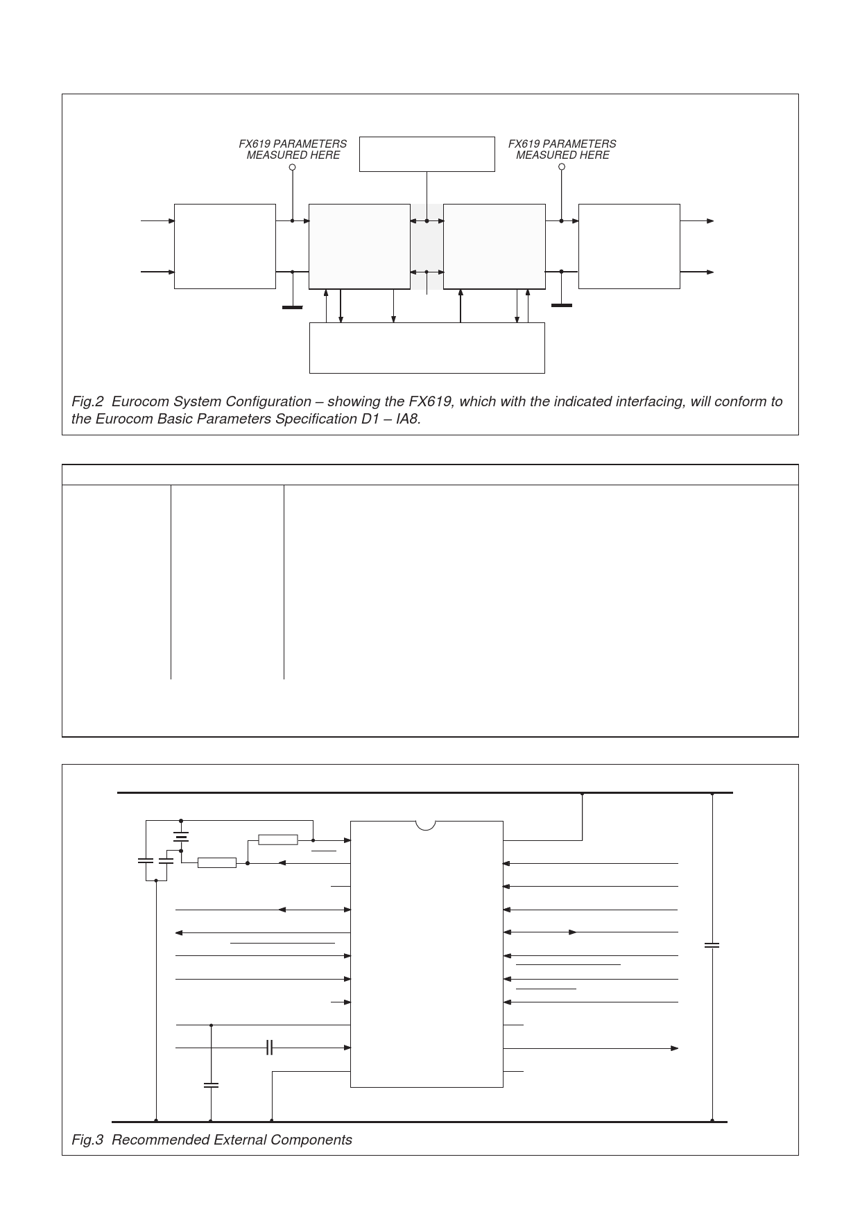
FX619 PARAMETERS
MEASURED HERE
REGULATED POWER
SUPPLY
FX619 PARAMETERS
MEASURED HERE
EUROCOM
INPUT
EUROCOM
ANALOGUE
INPUT
INTERFACE
(BALUN
&
BUFFER)
FX619
ENCODER
FX619
DECODER
DATA
CLOCKS
CLOCK MODE DATA
16/32/64kb/s
CLOCKS
1.024 MHz
SYNCHRONOUS CLOCK
AND
DATA SYSTEM
1.024 MHz
EUROCOM
ANALOGUE
OUTPUT
INTERFACE
(BALUN
&
BUFFER)
EUROCOM
OUTPUT
Fig.2 Eurocom System Configuration – showing the FX619, which with the indicated interfacing, will conform to
the Eurocom Basic Parameters Specification D1 – IA8.
Component
R1
R2
C
1
C2
C3
C4
C
5
X1
Unit Value
1M
Selectable
33p
33p
1.0µ
1.0µ
1.0µ
1.024 MHz
Note – with reference to Figure 3 (below)
Oscillator Inverter bias resistor.
Xtal Drive limiting resistor.
Xtal Circuit drain capacitor.
Xtal Circuit gate capacitor.
Encoder Input coupling capacitor – The drive source impedance to this
input should be less than 100Ω. Output Idle channel noise levels will
improve with an even lower source impedance.
Bias decoupling capacitor.
V decoupling capacitor.
DD
A 1.024 MHz Xtal/clock input will yield exactly 16/32/64 kb/s data clock
rates. Xtal circuitry shown is in accordance with CML application note
D/XT/1 April 1986.
Tolerance :– Resistors ± 10% Capacitors ± 20%
VDD
XTAL/CLOCK
X1
C2
C1
R2
1
R1
XTAL
2
N/C
3
VDD
22
CLOCK MODE 1
21
CLOCK MODE 2
20
ENCODER DATA CLOCK
4
ALGORITHM
19
ENCODER OUTPUT
5
DECODER DATA CLOCK
18
ENCODER FORCE IDLE
6
FX619J
DECODER INPUT
17
C5
DATA ENABLE
7
DECODER FORCE IDLE
16
N/C
8
POWERSAVE
15
BIAS
9
ENCODER INPUT
10
C3
11
C4
VSS
N/C
14
DECODER OUTPUT
13
N/C
12
Fig.3 Recommended External Components
V SS
4
Share Link: 