FX619 データシートの表示(PDF) - CML Microsystems Plc
部品番号
コンポーネント説明
一致するリスト
FX619 Datasheet PDF : 11 Pages
| |||
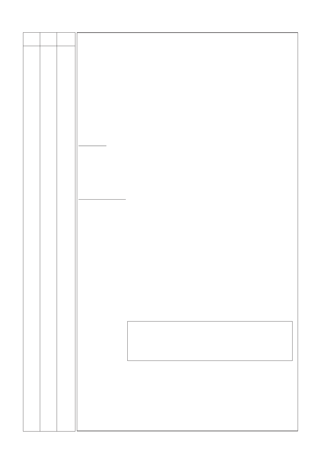
Pin Number Function
FX619 FX619 FX619
J L1/L2 M1
12 13 15,16 No connection
13 14 17 Decoder Output : The recovered analogue signal is output at this pin, it is the buffered
output of a bandpass filter and requires external components. During "Powersave" this
output is o/c.
14 15 18,19 No connection
15 16 20 Powersave : A logical '0' at this pin puts most parts of the codec into a quiescent non-
operational state. When at a logical '1' the codec operates normally. Internal 1MΩ Pullup.
17 21 No connection
16 18 22 Decoder Force Idle : A logical '0' at this pin gates a 0101...pattern internally to the
decoder so that the decoder output goes to VDD/2. When this pin is at a logical '1' the
decoder operates as normal. Internal 1MΩ Pullup.
17 19 23 Decoder Input : The received digital signal input. Internal 1MΩ Pullup.
18 20 24 Decoder Data Clock : A Logic I/O port. External decode clock input or internal data clock
output, dependant upon clock mode 1, 2 inputs, see Clock Mode pins.
19 21 25 Algorithm : A logical '1' at this pin sets this device for a 3-bit companding algorithm. A
logical '0' sets a 4-bit companding algorithm. Internal 1MΩ Pullup.
20 22 26 Clock Mode 2 :
21 23 27 Clock Mode 1 :
Internal 1MΩ
Pullups.
Clock Mode 1
0
0
1
1
Clock Mode 2
0
1
0
1
Facility
External clocks
Internal, 64kb/s = f ÷ 16
Internal, 32kb/s = f ÷ 32
Internal, 16kb/s = f ÷ 64
Clock rates refer to f = 1.024 MHz Xtal/clock input. During internal operation the data
clock frequencies are available at the ports for external circuit synchronization.
Independant or common data rate inputs to Encode and Decode data clock ports may be
employed in the External Clocks mode.
22 24 28 V : Positive Supply. A single + 5 volt power supply is required.
DD
3
Share Link: 