ADM1014 データシートの表示(PDF) - Analog Devices
部品番号
コンポーネント説明
一致するリスト
ADM1014 Datasheet PDF : 12 Pages
| |||
PRELIMINARY TECHNICAL DATA
ADM1014
the capacitor on 12VG, the +3.3VAUX, 3.3V and 5V outputs
may not have exceeded their undervoltage thresholds by the
time the undervoltage comparators are enabled, and a false
undervoltage condition may be detected. For this reason it is
recommended to use the same value for all three gate capaci-
tors.
For PCI applications the minimum recommended value is
0.033µF. Smaller values may cause overcurrent faults at power-
up due to excessive charging currents drawn by decoupling
capacitors.
The maximum value of the gate capacitors is determined by the
need to discharge them quickly when turning off the outputs
under fault conditions. If the capacitors are too large the
ADM1014 may be unable to protect the power bus or the ex-
ternal MOSFETs. With 0.033µF capacitors, the turn-off time
will be less than 6µs.
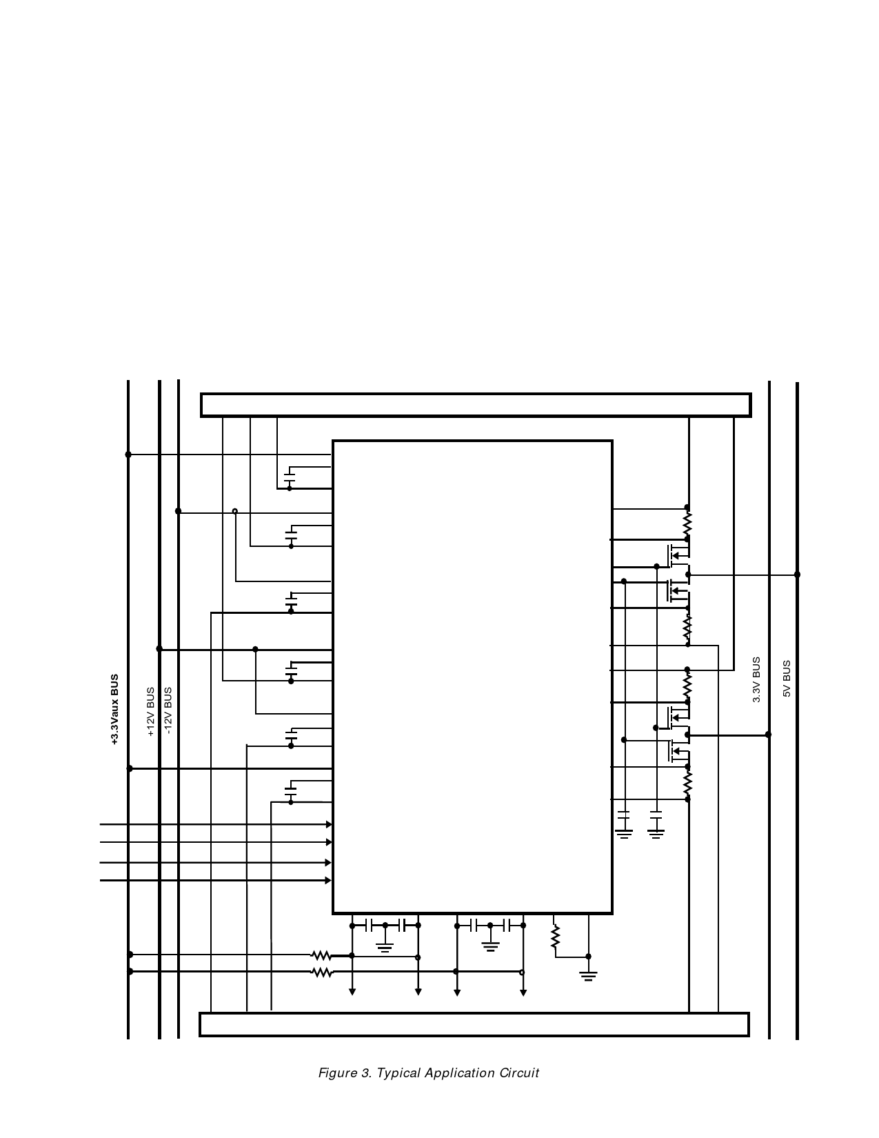
APPLICATIONS INFORMATION
APPLICATION CIRCUIT
Figure 3 shows a typical circuit configuration for the ADM1014 in
a PCI application, controlling supply voltages of +3.3V at up to
7.6A, +5V at up to 5A, +12V at up to 0.5A and –12V at up to
0.1A. In this circuit, two external MOSFETs are connected in
parallel for the 3.3V and 5V outputs to minimise on-resistance.
12V -12V +3.3Vaux
SLOT 1
5V
3.3V
FROM
SYSTEM
CONTROLLER
AUXINA
AUXGA
C1
AUXOA
M12VINA
M12GA
C2
M12VOA
M12VINB
M12GB
C3
M12VOB
5VISENA
5VSA
3V5VGA
3V5VGB
5VSB
12VINA
12VGA
C4
12VOA
12VINB
12VGB
C5
12VOB
ADM1014
5VISENB
3VISENA
3VSA
AUXINB
AUXGB
C6
AUXOB
3VSB
3VISENB
PAUXONA
PWRONA
PWRONB
PAUXONB
FLTNA FAUXA FLTNB
FAUXB OCSET GND
R11
C9 C10
C11 C12 R5
R1
Q1
Q2
R2
R3
Q3
Q4
R4
C7 C8
R12
12V -12V +3.3Vaux
TO SYSTEM CONTROLLER
SLOT 2
3.3V 5V
Figure 3. Typical Application Circuit
–10–
REV. PrN 1/02
Share Link: 