MPC9100FA データシートの表示(PDF) - Motorola => Freescale
部品番号
コンポーネント説明
一致するリスト
MPC9100FA Datasheet PDF : 8 Pages
| |||
MPC9100
MPC9100
OUTPUT
BUFFER
IN
7Ω
RS = 43Ω ZO = 50Ω
OutA
MPC9100
OUTPUT
BUFFER
IN
7Ω
RS = 43Ω ZO = 50Ω
RS = 43Ω ZO = 50Ω
OutB0
OutB1
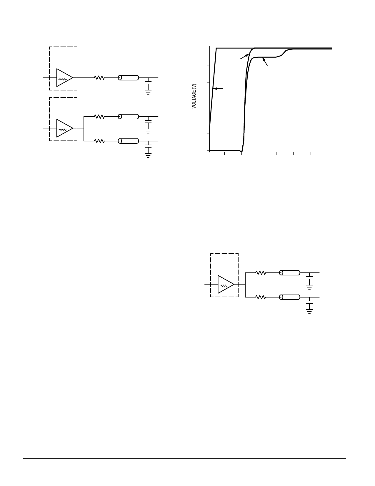
Figure 3. Single versus Dual Transmission Lines
The waveform plots of Figure 4 show the simulation
results of an output driving a single line vs two lines. In both
cases the drive capability of the MPC9100 output buffers is
more than sufficient to drive 50Ω transmission lines on the
incident edge. Note from the delay measurements in the
simulations a delta of only 43ps exists between the two
differently loaded outputs. This suggests that the dual line
driving need not be used exclusively to maintain the tight
output–to–output skew of the MPC9100. The output
waveform in Figure 4 shows a step in the waveform, this step
is caused by the impedance mismatch seen looking into the
driver. The parallel combination of the 43Ω series resistor
plus the output impedance does not match the parallel
combination of the line impedances. The voltage wave
launched down the two lines will equal:
VL = VS ( Zo / (Rs + Ro +Zo))
Zo = 50Ω || 50Ω
Rs = 43Ω || 43Ω
Ro = 7Ω
VL = 3.0 (25 / (21.5 + 7 + 25) = 3.0 (25 / 53.5)
= 1.40V
At the load end the voltage will double, due to the near
unity reflection coefficient, to 2.8V. It will then increment
towards the quiescent 3.0V in steps separated by one round
trip delay (in this case 4.0ns).
3.0
OutA
2.5
tD = 3.8956
2.0
In
1.5
OutB
tD = 3.9386
1.0
0.5
0
2
4
6
8
10 12 14
TIME (nS)
Figure 4. Single versus Dual Waveforms
Since this step is well above the threshold region it will not
cause any false clock triggering, however designers may be
uncomfortable with unwanted reflections on the line. To
better match the impedances when driving multiple lines the
situation in Figure 5 should be used. In this case the series
terminating resistors are reduced such that when the parallel
combination is added to the output buffer impedance the line
impedance is perfectly matched.
MPC9100
OUTPUT
BUFFER
7Ω
RS = 36Ω ZO = 50Ω
RS = 36Ω ZO = 50Ω
7Ω + 36Ω k 36Ω = 50Ω k 50Ω
25Ω = 25Ω
Figure 5. Optimized Dual Line Termination
SPICE level output buffer models are available for
engineers who want to simulate their specific interconnect
schemes. In addition IV characteristics are in the process of
being generated to support the other board level simulators in
general use.
MOTOROLA
6
TIMING SOLUTIONS
BR1333 — REV 5
Share Link: 