MPC9100FA データシートの表示(PDF) - Motorola => Freescale
部品番号
コンポーネント説明
一致するリスト
MPC9100FA Datasheet PDF : 8 Pages
| |||
MPC9100
Figure 2 illustrates a typical power supply filter scheme.
The MPC9100 is most susceptible to noise with spectral
content in the 1KHz to 1MHz range. Therefore the filter
should be designed to target this range. The key parameter
that needs to be met in the final filter design is the DC voltage
drop that will be seen between the VCC supply and the VCCA
pin of the MPC9100. The current into the VCCA pin is
typically 15mA (20mA maximum), assuming that a minimum
of 3.0V must be maintained on the PLL_VCC pin very little
DC voltage drop can be tolerated when a 3.3V VCC supply is
used. The resistor shown in Figure 2 must have a resistance
of 10–15Ω to meet the voltage drop criteria. The RC filter
pictured will provide a broadband filter with approximately
100:1 attenuation for noise whose spectral content is above
20KHz. As the noise frequency crosses the series resonant
point of an individual capacitor it’s overall impedance begins
to look inductive and thus increases with increasing
frequency. The parallel capacitor combination shown
ensures that a low impedance path to ground exists for
frequencies well above the bandwidth of the PLL.
A higher level of attenuation can be achieved by replacing
the resistor with an appropriate valued inductor. A 1000µH
choke will show a significant impedance at 10KHz
frequencies and above. Because of the current draw and the
voltage that must be maintained on the PLL_VCC pin a low
DC resistance inductor is required (less than 15Ω). Generally
the resistor/capacitor filter will be cheaper, easier to
implement and provide an adequate level of supply filtering.
Although the MPC9100 has several design features to
minimize the susceptibility to power supply noise (isolated
power and grounds and fully differential PLL) there still may
be applications in which overall performance is being
degraded due to system power supply noise. The power
supply filter schemes discussed in this section should be
adequate to eliminate power supply noise related problems
in most designs.
Using the On–Board Crystal Oscillator
The MPC9100 features an on–board crystal oscillator to
allow for seed clock generation as well as final distribution.
The on–board oscillator is completely self contained so that
the only external component required is the crystal. As the
oscillator is somewhat sensitive to loading on its inputs the
user is advised to mount the crystal as close to the MPC9100
as possible to avoid any board level parasitics. To facilitate
co–location surface mount crystals are recommended, but
not required. In addition, with crystals with a higher shunt
capacitance, it may be necessary to place a 1k resistor
across the two crystal leads.
The oscillator circuit is a series resonant circuit as
opposed to the more common parallel resonant circuit, this
eliminates the need for large on–board capacitors. Because
the design is a series resonant design for the optimum
frequency accuracy a series resonant crystal should be used
(see specification table below). Unfortunately most off the
shelf crystals are characterized in a parallel resonant mode.
However a parallel resonant crystal is physically no different
than a series resonant crystal, a parallel resonant crystal is
simply a crystal which has been characterized in its parallel
resonant mode. Therefore in the majority of cases a parallel
specified crystal can be used with the MPC9100 with just a
minor frequency error due to the actual series resonant
frequency of the parallel resonant specified crystal. Typically
a parallel specified crystal used in a series resonant mode
will exhibit an oscillatory frequency a few hundred ppm lower
than the specified value. For most processor
implementations a few hundred ppm translates into kHz
inaccuracies, a level which does not represent a major issue.
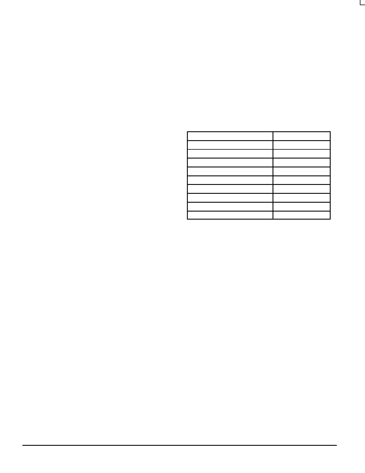
Table 1. Crystal Specifications
Parameter
Value
Crystal Cut
Fundamental AT Cut
Resonance
Series Resonance*
Frequency Tolerance
±75ppm at 25°C
Frequency/Temperature Stability
±150pm 0 to 70°C
Operating Range
0 to 70°C
Shunt Capacitance
5–7pF
Equivalent Series Resistance (ESR) 50 to 80Ω
Correlation Drive Level
100µW
Aging
5ppm/Yr (First 3 Years)
* See accompanying text for series versus parallel resonant
discussion.
Driving Transmission Lines
The MPC9100 clock driver was designed to drive high
speed signals in a terminated transmission line environment.
To provide the optimum flexibility to the user the output
drivers were designed to exhibit the lowest impedance
possible. With an output impedance of less than 10Ω the
drivers can drive either parallel or series terminated
transmission lines. For more information on transmission
lines the reader is referred to application note AN1091 in the
Timing Solutions brochure (BR1333/D).
In most high performance clock networks point–to–point
distribution of signals is the method of choice. In a
point–to–point scheme either series terminated or parallel
terminated transmission lines can be used. The parallel
technique terminates the signal at the end of the line with a
50Ω resistance to VCC/2. This technique draws a fairly high
level of DC current and thus only a single terminated line can
be driven by each output of the MPC9100 clock driver. For
the series terminated case however there is no DC current
draw, thus the outputs can drive multiple series terminated
lines. Figure 3 illustrates an output driving a single series
terminated line vs two series terminated lines in parallel.
When taken to its extreme the fanout of the MPC9100 clock
driver is effectively doubled due to its capability to drive
multiple lines.
TIMING SOLUTIONS
5
BR1333 — REV 5
MOTOROLA
Share Link: 