UPD72852 データシートの表示(PDF) - NEC => Renesas Technology
部品番号
コンポーネント説明
一致するリスト
UPD72852 Datasheet PDF : 48 Pages
| |||
µPD72852
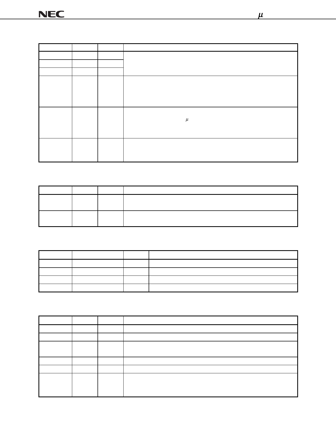
1.3 Control Pins
Name
PC0
PC1
PC2
CMC
Pin No.
26
27
28
30
RESETB
55
SPD
61
I/O
Function
I
Power class set input
I
This pin status will be loaded to Pwr_class bit which allocated to PHY register 4H.
I
IEEE1394a-2000 chapter [4.3.4.1]
I
Configuration manager capable setting
This pin status will be loaded to Contender bit which allocated to PHY register 4H.
0: Non contender
1: Contender
I
Power-on reset input
Connect to GND through a 0.1 µF capacitor.
0: Reset
1: Normal
I
Speed select
0: MAX. S200
1: MAX. S400
1.4 IC
Name
IC(AL)
Pin No.
29, 51
IC(DL)
3
I/O
Function
-
Internally Connected (Low Clamped)
Connect to GND.
-
Internally Connected (Low Clamped)
Connect to GND.
1.5 Power Supply Pins
Name
AVDD
AGND
DVDD
DGND
Pin No.
I/O
25, 31, 40, 47, 54
-
24, 33, 35, 42, 49, 52, 53
-
4, 10, 20, 56, 60
-
1, 7, 13, 16, 21, 57, 64
-
Analog power
Analog GND
Digital VDD
Digital GND
Function
1.6 Other Pins
Name
TpBias0
TpBias1
RI1
Pin No.
41
48
34
XI
23
XO
22
TEST
62
I/O
Function
O
Port 0 twisted pair output
O
Port 1 twisted pair output
-
Resistor connection pin1 for reference current generator
Connect to GND through a 9.1 kΩ resistor.
-
Crystal oscillator connection XI
-
Crystal oscillator connection XO
-
Test pin
Internally connected (Low clamped).
Connect to GND.
8
Data Sheet S14920EJ3V0DS
Share Link: 