UPD72873 データシートの表示(PDF) - NEC => Renesas Technology
部品番号
コンポーネント説明
一致するリスト
UPD72873 Datasheet PDF : 40 Pages
| |||
µPD72873
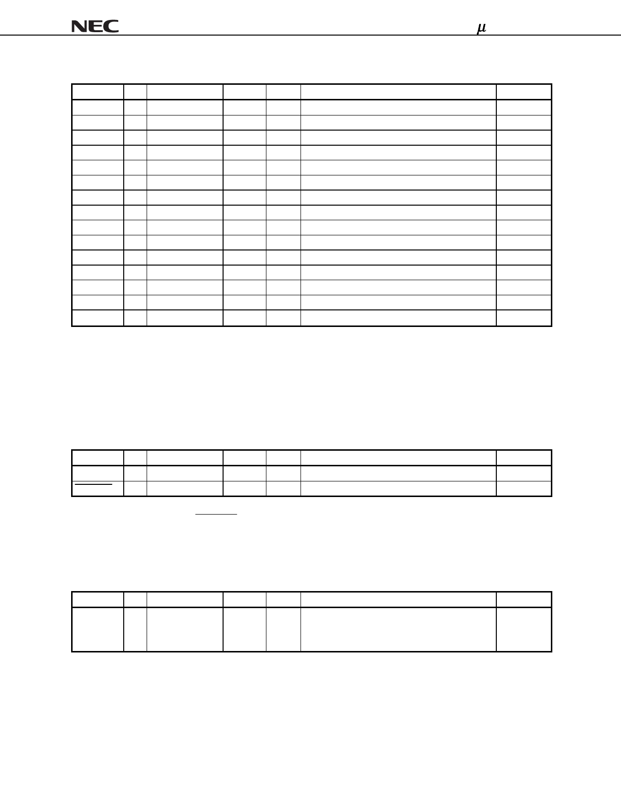
1.2 PHY Signals: (15 pins)
Name
TpA0p
TpA0n
TpB0p
TpB0n
TpA1p
TpA1n
TpB1p
TpB1n
CPS
TpBias0
TpBias1
RI0
RI1
XI
XO
I/O
Pin No.
I/O 101
I/O 100
I/O 99
I/O 98
I/O 105
I/O 104
I/O 103
I/O 102
I 93
O 96
O 97
- 91
- 92
I 87
O 88
IOL
Volts(V)
Function
Block *
-
- Port-1 Twisted Pair A Positive Input/Output Note 1 PHY Analog
-
- Port-1 Twisted Pair A Negative Input/Output Note 1 PHY Analog
-
- Port-1 Twisted Pair B Positive Input/Output Note 1 PHY Analog
-
- Port-1 Twisted Pair B Negative Input/Output Note 1 PHY Analog
-
- Port-2 Twisted Pair A Positive Input/Output Note 1 PHY Analog
-
- Port-2 Twisted Pair A Negative Input/Output Note 1 PHY Analog
-
- Port-2 Twisted Pair B Positive Input/Output Note 1 PHY Analog
-
- Port-2 Twisted Pair B Negative Input/Output Note 1 PHY Analog
-
-
Cable Power Status Input Note2
PHY Digital
-
-
Port-1 Twisted Pair Bias Voltage Output Note 1
PHY Analog
-
-
Port-2 Twisted Pair Bias Voltage Output Note 1
PHY Analog
-
-
Resistor0 for Reference Current Setting Note 3
PHY Analog
-
- Resistor1 for Reference Current Setting Note 3
PHY Analog
-
- X’tal XI
PHY Analog
-
- X’tal XO
PHY Analog
Notes 1. If unused port, please refer to 4.1.4 Unused Ports.
2. Please refer to 4.1.3 CPS.
3. Please refer to 4.5 RI0, RI1.
Remark *: If the PHY Digital pin is pulled up, it should be connected to P_DVDD.
If the PHY Analog pin is pulled up, it should be connected to P_AVDD.
1.3 PHY Control Signals: (4 pins)
Name
I/O
Pin No.
IOL
PC0 to PC2 I 70 to 72
-
P_RESET
I 81
-
Notes 1. Please refer to 4.3 PC0 to PC2.
2. Please refer to 4.4 P_RESET.
Volts(V)
Function
3.3 Power Class Input Note 1
-
PHY Power on Reset Input Note 2
Block *
PHY Digital
PHY Digital
Remark *: If the PHY Digital pin is pulled up, it should be connected to P_DVDD.
1.4 PCI/Cardbus Select Signal: (1 pin)
Name
I/O
Pin No.
IOL
Volts(V)
Function
CARD_ON I 119
-
3.3 PCI/CardBus Select
1:Cardbus mode
0:PCI bus mode
Remark *: If the Link pin is pulled up, it should be connected to L_VDD.
Block *
Link
10
Preliminary Data Sheet S15305EJ2V0DS
Share Link: 