1400 データシートの表示(PDF) - Linear Technology
部品番号
コンポーネント説明
一致するリスト
1400 Datasheet PDF : 20 Pages
| |||
LTC1400
APPLICATIO S I FOR ATIO
trimmed to 2.42V. It is internally connected to the DAC
and is available at Pin 3 to provide up to 1mA of current to
an external load. For minimum code transition noise, the
reference output should be decoupled with a capacitor to
filter wideband noise from the reference (10μF tantalum in
parallel with a 0.1μF ceramic). The VREF pin can be driven
with a DAC or other means to provide input span adjust-
ment in bipolar mode. The VREF pin must be driven to at
least 2.45V to prevent conflict with the internal reference.
The reference should not be driven to more than 5V.
Figure 6 shows an LT1360 op amp driving the reference
pin. Figure 7 shows a typical reference, the LT1019A-5
connected to the LTC1400. This will provide an improved
drift (equal to the maximum 5ppm/°C of the LT1019A-
5) and a ±4.231V full scale. If VREF is forced lower than
2.42V, the REFRDY bit in the serial data output will be
forced to low.
INPUT RANGE
±0.846 • VREF(OUT)
+
LT1360
–
VREF(OUT) ≥ 2.45V
3Ω
10µF
5V
AIN VCC
LTC1400
VREF
GND VSS
–5V
1400 F06
Figure 6. Driving the VREF with the LT1360 Op Amp
INPUT RANGE ±4.231V
(= ±0.846 • VREF)
10V
VIN
VOUT
LT1019A-5
GND
3Ω
10µF
5V
AIN VCC
LTC1400
VREF
GND VSS
–5V
1400 F07
Figure 7. Supplying a 5V Reference Voltage
to the LTC1400 with the LT1019A-5
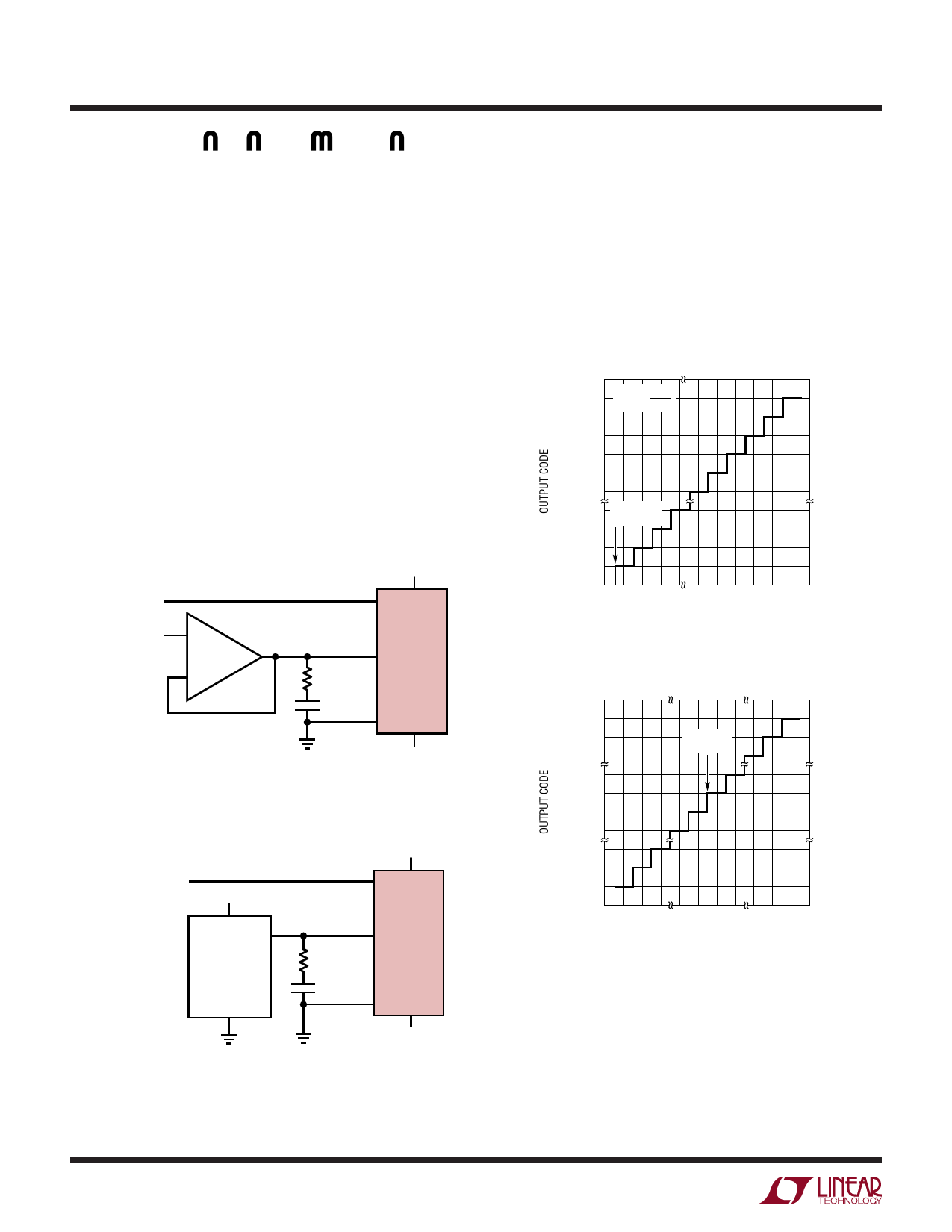
Unipolar/Bipolar Operation and Adjustment
Figure 8 shows the ideal input/output characteristics for
the LTC1400. The code transitions occur midway between
successive integer LSB values (i.e., 0.5LSB, 1.5LSB,
2.5LSB, … FS – 1.5LSB). The output code is straight
binary with 1LSB = 4.096V/4096 = 1mV. Figure 9 shows
the input/output transfer characteristics for the bipolar
mode in two’s complement format.
111...111
111...110
111...101
111...100
1LSB
=
FS
4096
UNIPOLAR
ZERO
000...011
000...010
000...001
000...000
0V 1
LSB
INPUT VOLTAGE (V)
FS – 1LSB
1400 F08
Figure 8. LTC1400 Unipolar Transfer Characteristics
011...111
011...110
000...001
000...000
111...111
111...110
BIPOLAR
ZERO
100...001
100...000
– FS/2
–1 0V 1
LSB LSB
INPUT VOLTAGE (V)
FS/2 – 1LSB
11400 F09
Figure 9. LTC1400 Bipolar Transfer Characteristics
Unipolar Offset and Full-Scale Error Adjustments
In applications where absolute accuracy is important,
offset and full-scale errors can be adjusted to zero. Figure
10a shows the extra components required for full-scale
1400fa
10
Share Link: 