SS6620 データシートの表示(PDF) - Silicon Standard Corp.
部品番号
コンポーネント説明
一致するリスト
SS6620 Datasheet PDF : 12 Pages
| |||
n ELECTRICAL CHARACTERISTICS (Continued)
SS6620/21/2
PARAMETER
LBI Input Current
CLSEL Input Current
SHDN Input Current
LBO Low Output Voltage
LBO Off Leakage Current
LBI Hystereisis
Damping Switch Resistance
TEST CONDITIONS
VLBI = 1.4V
SS6622 , CLSEL = OUT
V SHDN = 0 or VOUT
VLBI = 0, ISINK = 1mA
VLBO = 5.5V, VLBI = 5.5V
SS6622, VBATT = 2V
SHDN Input Voltage
CLSEL Input Voltage
MIN. TYP. MAX. UNIT
1
50
nA
1.4
3
µA
0.07
50
nA
0.2
0.4
µA
0.07
1
50
mV
50
100
Ω
0.8VOUT
0.2VOUT
V
0.8VOUT
0.2VOUT
V
Note 1: Start-up voltage operation is guaranteed without the addition of an external Schottky diode between the in-
put and output.
Note 2: Steady-state output current indicates that the device maintains output voltage regulation under load.
Note 3: Device is bootstrapped (power to the IC comes from OUT). This correlates directly with the actual battery
supply.
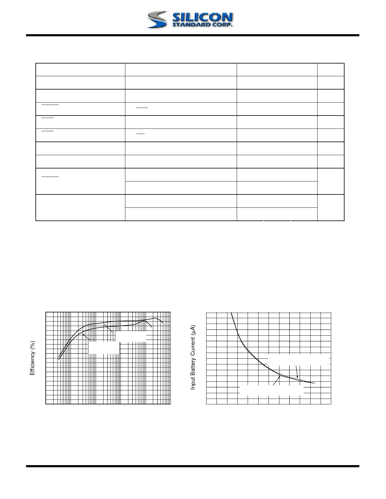
n TYPICAL PERFORMANCE CHARACTERISTICS
100
90
80
70
VIN=2.4V
60
VIN=1.2V
50
40
30
20
10
0
0.01
0.1
1
10
100
1000
Loading (mA)
Fig. 1 VOUT=3.3V CLSEL=OUT (0.8A)
160
140
120
100
80
I_limit=0.8A , VOUT=3.3V
60
40
20
I_limit=0.45A , VOUT=3.3V
0 0.0
0.5
1.0
1.5
2.0
2.5
3.0
Input battery voltage (V)
Fig. 2 No-Load Battery Current vs. Input Battery Voltage
Rev.2.01 6/06/2003
www.SiliconStandard.com
4 of 12
Share Link: 