SS6620 データシートの表示(PDF) - Silicon Standard Corp.
部品番号
コンポーネント説明
一致するリスト
SS6620 Datasheet PDF : 12 Pages
| |||
Component Selection
1. Inductor Selection
An inductor value of 22µH performs well in most
applications. The SS6620 series also work
with inductors in the 10µH to 47µH range. An in-
ductor with higher peak inductor current creates a
higher output voltage ripple (IPEAK output filter ca-
pacitor ESR). The inductor’s DC resistance sig-
nificantly affects efficiency. We can calculate the
maximum output current as follows:
I OUT(MAX )
=
VIN
VOUT
ILIM
−
t
OFF
VOUT − VIN
2×L
η
where IOUT(MAX)=maximum output current in amps
VIN=input voltage
L=inductor value in µH
? =efficiency (typically 0.9)
tOFF=LX switch’ off-time in µS
ILIM=0.45A or 0.8A
2. Capacitor Selection
The output voltage ripple is related to the peak in-
ductor current and the output capacitor ESR. Be-
sides output ripple voltage, the output ripple cur-
rent also needs to be considered. The smaller the
ESR of the output capacitor, the higher the ripple
current. A filter capacitor with low ESR is helpful
SS6620/21/2
to the efficiency and steady state output current of
the SS6620 series. Therefore HERMEI ca-
pacitor LT series with 220µF/6.3V is recom-
mended. A smaller capacitor (down to 10µF with
higher ESR) is acceptable for light loads or in ap-
plications that can tolerate higher output ripple.
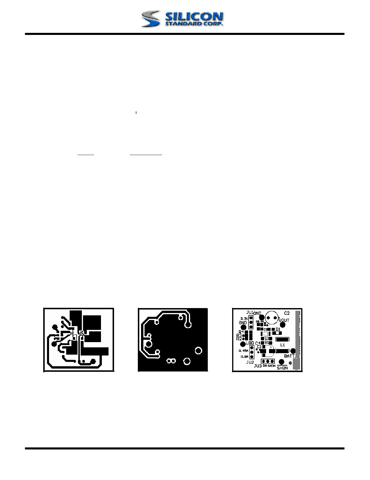
3. PCB Layout and Grounding
Since the SS6622’s switching frequency can
range up to 500kHz, the SS6622 can be very
sensitive. Careful printed circuit layout is impor-
tant for minimizing ground bounce and noise. The
area around the IC’s OUT pin should be as clear
as possible, and the GND pin should be placed
close to the ground plane. Keep the IC’s GND pin
and the ground leads of the input and output filter
capacitors less than 0.2in (5mm) apart. In addition,
keep all connections to the FB and LX pins as
short as possible. In particular, when using exter-
nal feedback resistors, locate them as close to the
FB pin as possible. To maximize output power
and efficiency and minimize output ripple voltage,
use a ground plane and solder the IC’s GND di-
rectly to the ground plane. Following are the rec-
ommended layout diagrams.
Figure 12. Top layer
Figure 13. Bottom layer
Figure 14. Placement
Rev.2.01 6/06/2003
www.SiliconStandard.com
10 of 12
Share Link: 