PA7536 データシートの表示(PDF) - Anachip Corporation
部品番号
コンポーネント説明
一致するリスト
PA7536 Datasheet PDF : 10 Pages
| |||
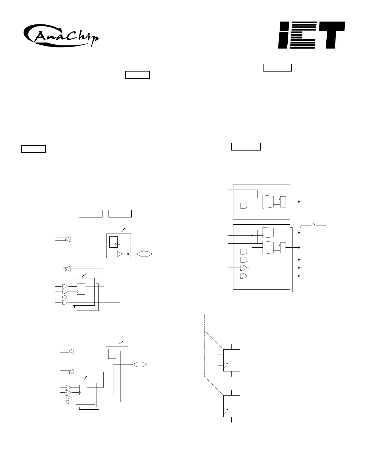
Input Cells (INC)
Input cells (INC) are included on dedicated input pins. The
block diagram of the INC is shown in Figure 6. Each INC
consists of a multiplexer and a register/transparent latch,
which can be clocked from various sources selected by the
global cell. The register is rising edge clocked. The latch is
transparent when the clock is high and latched on the
clock’s failing edge. The register/latch can also be
bypassed for a non registered input.
I/O Cell (IOC)
All PEEL™ Arrays have I/O cells (IOC) as shown above in
Figure 6. Inputs to the IOCs can be fed from any of the
LCCs in the array. Each IOC consists of routing and control
multiplexers, an input register/transparent latch, a three-
state buffer and an output polarity control. The register/
latch can be clocked from a variety of sources determined
by the global cell. It can also be bypassed for a non-
registered input. A feature of the 7536 IOC is the use of
SUM-D as a feed-back to the array when the I/O pin is a
dedicated output. This allows for additional buried registers
and logic paths. (See Figure 8 & Figure 9).
Global Cells
The global cells, shown in Figure 10, are used to direct
global clock signals and/or control terms to the LCCs, IOCs
and INCs. The global cells allow a clock to be selected
from the CLK1 pin, CLK2 pin, or a product term from the
logic array (PCLK). They also provide polarity control for
IOC clocks enabling rising or falling clock edges for input
registers/latches. Note that each individual LCC clock has
its own polarity control. The global cell includes sum-of-
products control terms for global reset and preset, and a
fast product term control for LCC register-type, used to
save product terms for loadable counters and state
machines (see Figure 11). The PA7536 provides two
global cells that divide the LCC and IOCs into two groups,
A and B. Half of the LCCs and IOCs use global cell A, half
use global cell B. This means, for instance, two high-speed
global clocks can be used among the LCCs.
CLK1
CLK2
PCLK
MUX
Global Cell: INC
INC Clocks
Group A & B
QD
Input with optional
register/latch
I/O
1
A
DQ
B
2
C
D
OE
I/O with
independent
output enable
08-16-008A
Figure 8. LCC & IOC With Two Outputs
CLK1
CLK2
PCLK
Reg-Type
Preset
Reset
MUX
MUX
Global Cell: LCC & IOC
Figure 10. Global Cells
Reg-Type from Global Cell
LCC Clocks
IOC Clocks
LCC Reg-Type
LCC Presets
LCC Resets
08-16-010A
QD
Buried register or
logic paths
O utp u t
1
A
DQ
B
C
2
D
3
08-16-009A
Figure 9. LCC & IOC With Three Outputs
4
P
D
Q
R
Register Type Change Feature
Global Cell can dynamically change user-
selected LCC registers from D to T or from D
to JK. This saves product terms for loadable
counters or state machines. Use as D register
to load, use as T or JK to count. Timing allows
dynamic operation.
P
T
Q
R
Exam ple:
Product terms for 10 bit loadable binary counter
D uses 57 product terms (47 count, 10 load)
T uses 30 product terms (10 count, 20 load)
D/T uses 20 product terms (10 count, 10 load)
08-16-011A
Figure 11. Register Type Change Feature
04-02-052A
Share Link: 