OM6206 データシートの表示(PDF) - Philips Electronics
部品番号
コンポーネント説明
一致するリスト
OM6206 Datasheet PDF : 36 Pages
| |||
Philips Semiconductors
65 × 102 pixels matrix LCD driver
Product specification
OM6206
handbook, full pagewidth
09
1 10
2
3
4
5
6
7
8
0
X - address
0
Y-address
917
8
101
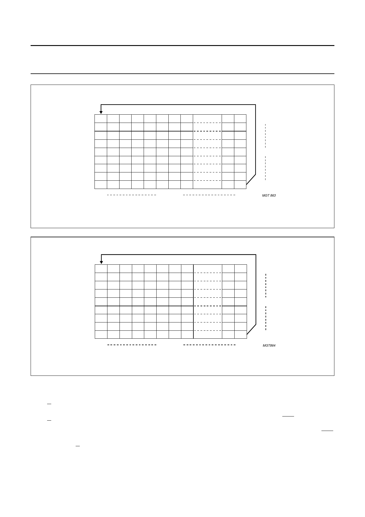
MGT 863
Fig.5 Sequence of writing data bytes into RAM with vertical addressing (V = 1).
handbook, full pagewidth
012
102 103 104
204 205 206
306 307 308
408 409 410
510 511 512
612 613 614
714 715 716
816 817 818
0
X - address
0
Y-address
917
8
101
MGT864
Fig.6 Sequence of writing data bytes into RAM with horizontal addressing (V = 0).
8 INSTRUCTIONS
The instruction format is divided into two modes:
• If D/C (mode select) is set LOW, the current byte is
interpreted as command byte (see Table 1).
• If D/C is set HIGH, the following bytes are stored in the
display data RAM. After every data byte the address
counter is incremented automatically.
The level of the D/C signal is read during the last bit of data
byte.
Every instruction can be sent in any order to the OM6206.
The MSB of a byte is transmitted first (see Fig.7). Figure 8
shows one possible command stream, used to set up the
LCD driver.
The serial interface is initialized when SCE is HIGH. In this
state SCLK clock pulses have no effect and no power is
consumed by the serial interface. A negative edge on SCE
enables the serial interface and indicates the start of a data
transmission.
2001 Nov 14
10
Share Link: 