NJU3505L データシートの表示(PDF) - Japan Radio Corporation
部品番号
コンポーネント説明
一致するリスト
NJU3505L Datasheet PDF : 64 Pages
| |||
NJU3505
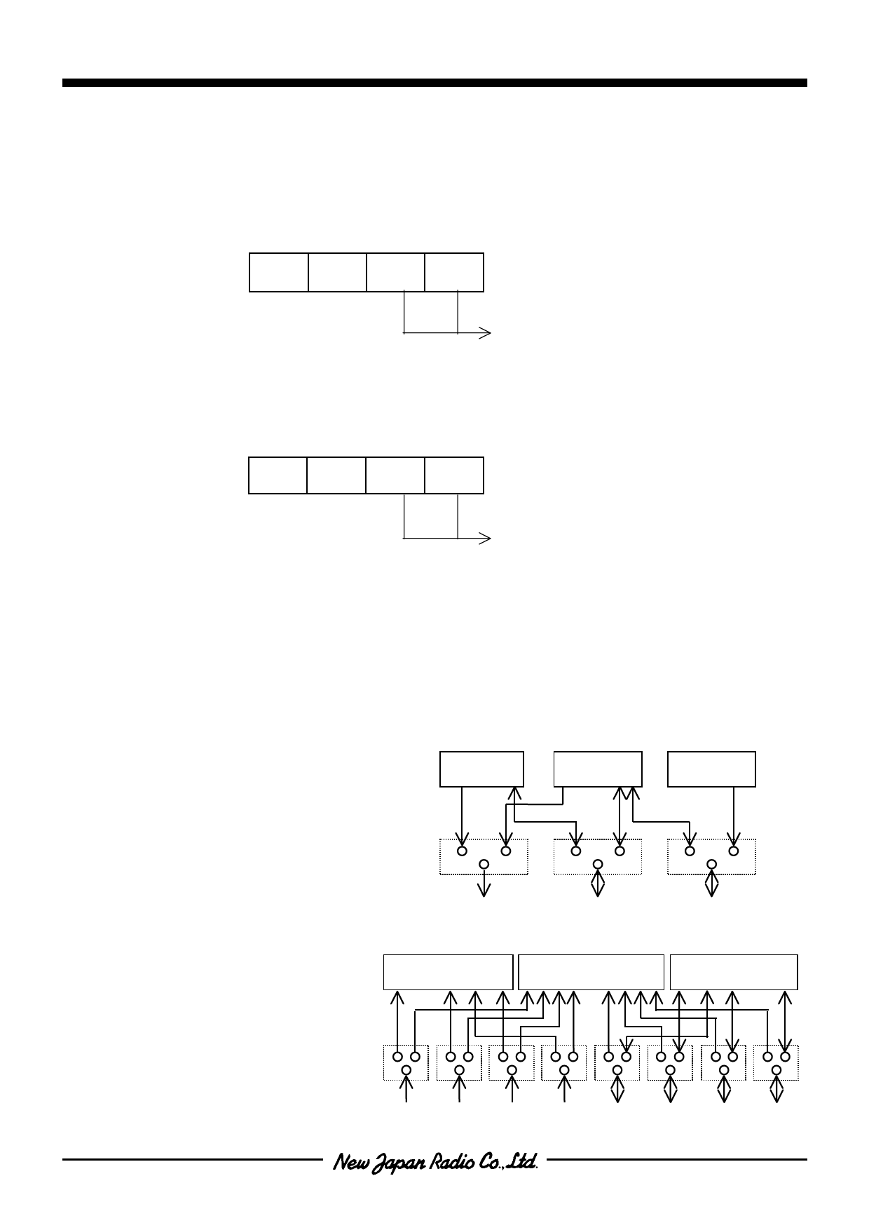
*2 Memory Bank Register(PHY15) selects the Bank0 in ROM when lower 2-bit of PHY15 is written “00”, and
selects the Bank1 when lower 2-bit of PHY15 is written “01”, and selects the Bank2 when lower 2-bit of
PHY15 is written “10”,and selects the Bank3 when lower 2-bit of PHY15 is written “11”.
The Bank0 is selected on “RESET” operation.
[ Reading from the Memory Bank Register (PHY15) ]
(MSB) 3
2
1
0 (LSB)
PHY15 “0”
“0”
[ Writing to Memory Bank Register (PHY15) ]
(MSB) 3
2
1
0
PHY15
−
−
Bank of ROM
/ 00:bank0
01:bank1
10:bank2
11:bank3
(LSB)
Note) Bank0 Address : 0000H − 07FFH,
Bank1 Address : 0800H − 0FFFH
Bank2 Address : 1000H − 17FFH
Bank3 Address : 1800H − 1FFFH
*3 Wiring of terminals
The mask option selects a terminal
type from SDO/PL0, SDI(O)/PL1 or
SCK/CKOUT as shown in right.
Bank of ROM
/ 00:bank0
01:bank1
10:bank2
11:bank3
PHY28
PHY2
Prescaler
*4 Wiring of terminals
The mask option selects a terminal
type from AIN0/PI0, AIN1/PI1,
AIN2/PI2, AIN3/PI3, AIN4/PA0,
AIN5/PA1, AIN6/PA2, AIN7/PA3
as shown in right.
SDO / PL0 SDI(O) / PL1 SCK / CKOUT
PHY25
ADC
PHY17
AIN0/PI0 AIN1/PI1 AIN2/PI2 AIN3/PI3 AIN4/PA0 AIN5/PA1 AIN6/PA2 AIN7/PA3
- 13 -
Share Link: 