NJU3503L データシートの表示(PDF) - Japan Radio Corporation
部品番号
コンポーネント説明
一致するリスト
NJU3503L Datasheet PDF : 60 Pages
| |||
NJU3503
s INPUT OUTPUT PORT
The NJU3503 prepares 8 Input-Output lines and 12 dual-function lines for the interface to an external
application circuit. All lines are assigned to each Peripheral Register.
Data reading operation from the peripheral register can input the actual signals through the input terminal.
Data writing operation to the peripheral register can output the actual signals through the output terminal.
[ PORT FUNCTION TABLE ]
PORT NAME
FUNCTION
INPUT/OUTPUT
PORTA
Input / Output port Programmable Input / Output PORT(4-bit).
PORTB
Input / Output port Input / Output selectable ports by the mask option.
PORTC(PC0)
Input port or ADCK Input
PORTC(PC1)
Input or VREF
PORTD
Input / Output port or
AIN0 − AIN3
PORTE(PE0,PE1)
Input / Output port or
AIN4 − AIN5
PORTE(PE2)
Input / Output port
Input
Input / Output selectable ports by the mask option
Input / Output selectable ports by the mask option.
Input / Output selectable ports by the mask option.
PORTF(PF0)
Input port or EXTI Input
PORTF(PF1)
Input port or CNTI Input
PORTG(PG0)
Output Port or SDO output
Input / Output port or
PORTG(PG1) SDI(O)
Input / Output selectable ports by the mask option.
Note1) Pull-up resistance is selected by the mask option.(refer !INPUT OUTPUT TERMINAL TYPE)
(1) INPUT OUTPUT PORT
• PORTA(PA0 − PA3)
PORTA is a 4-bit programmable input-output PORT. The input or the output is selected for each bit by
the programmable input/output control register (PHY24). It is set to “1” as the output, and is set to “0” as
the input. When the PORT is set as the output, the 4-bit signals are output through the output terminals by
writing data into the peripheral register assigned for PORTA (PHY17). PHY17 as the output register
should be written the output data before the PORTA is set as the output by PHY24, because the conditions
of the output terminals are unknown while the output data is not written in PHY17. When this PORT is set
as the input, the 4-bit external signals are gotten directly through the input terminals by reading data from
PHY17. PHY17 can be written or read independent of the state of PHY24 as the input or output.
Though the output circuit is Nch open drain type, the C-MOS input buffer is connected to the same
terminal. Therefore, the operating current of the chip by the short circuit current when the middle level
voltage between VDD and VSS is input to this terminal.
PORTA is set as the input in accordance with the state of PHY24 set to “0” on the “RESET” operation.
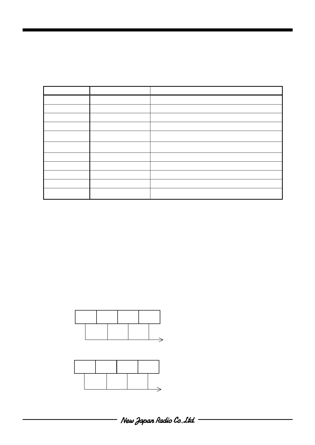
[ READING PORTA INPUT DATA (PHY17) ]
(MSB) 3
2
1
0 (LSB)
PHY17 PA3 PA2 PA1 PA0
PORTA Input Data
[ WRITING PORTA OUTPUT DATA (PHY17) ]
(MSB) 3
2
1
0 (LSB)
PHY17 PA3 PA2 PA1 PA0
PORTA Output Data
- 14 -
Share Link: 