NJU3502L データシートの表示(PDF) - Japan Radio Corporation
部品番号
コンポーネント説明
一致するリスト
NJU3502L Datasheet PDF : 42 Pages
| |||
NJU3502
• DATA MEMORY(RAM)
DATA MEMORY(RAM) is formed with the 4-bit length a word. The NJU3502 prepares 64 words(256
bits) RAM. The data formed with the 4-bit length a word can be read/written from/to RAM, and the data
formed with the 1-bit length in a word can be set, reset, or tested by the bit-operation instruction.
The RAM address is indicated indirectly by X- and Y-reg. The lower 2 bits(b0, b1) in X-reg are used as
the RAM address pointer and the higher 2 bits(b2, b3) are not used.
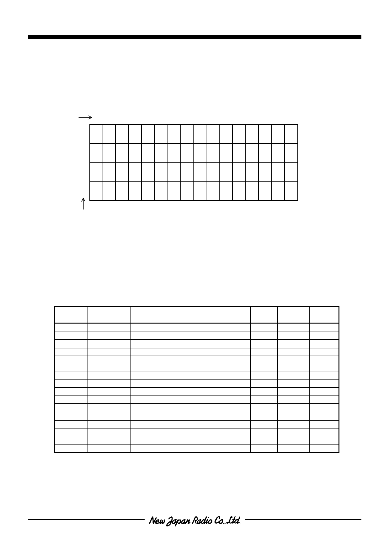
[RAM ADDRESS MAP]
Y-reg
0 1 2 3 4 5 6 7 8 9 A B C D E F [HEX]
0
1
2
3
[HEX]
X-reg
• PERIPHERAL REGISTERs(PH)
PERIPHERAL REGISTERs(PH) controlling I/O Ports or the ROM address are selected by the data in Y'-
reg.
The Peripheral Register assigned for each I/O Port can get the signal data from the external application
by reading operation, or can output the signal data to the external application by writing operation in
accordance with the type of input or output selected by the mask option. Although the data can be read
from the Peripheral Register assigned as the Output Port, it sometimes takes the incorrect data of the
Output Port.
[PERIPHERAL REGISTER TABLE]
Y'-register Register No.
Peripheral Register Name
0H PHY0 (00H)
1H PHY1 (01H) Serial Input/Output Control Register
2H PHY2 (02H) Serial Input/Output Shift Register
3H PHY3 (03H) Timer/Prescaler Control Register
4H PHY4 (04H) Initial Value Register / Timer Counter
5H PHY5 (05H) Interrupt Control Register
6H PHY6 (06H) PORTA Output or PORTA Input
7H PHY7 (07H) PORTB Output or PORTB Input
8H PHY8 (08H) PORTC Output or PORTC Input
9H PHY9 (09H) PORTD Output or PORTD Input
AH PHY10(0AH) PORTE Input
BH PHY11(0BH) PORTF Output or PORTF Input
CH PHY12(0CH) PORTB Input/Output Control Register
DH PHY13(0DH) ROM Addressing Register
EH PHY14(0EH)
FH PHY15(0FH)
Number Write or
of Port Read ∗1
3
WR
8
WR
3
WR
8
WR
3
WR
4
W or R
4
WR
4
W or R
2 / 3 W or R
1
R
2 / 1 W or R
1
WR
4
WR
Data in
Reset
0
0 ∗2
0 ∗2
0
0
0
0
0
0
0
0 ∗3
0 ∗2
0
unknown
∗1 W
R
WR
W or R
: Write only
: Read only
: Read and Write
: Fixed as Read or Write by the mask option
-8-
Share Link: 