NCV8668 データシートの表示(PDF) - ON Semiconductor
部品番号
コンポーネント説明
一致するリスト
NCV8668 Datasheet PDF : 21 Pages
| |||
NCV8668
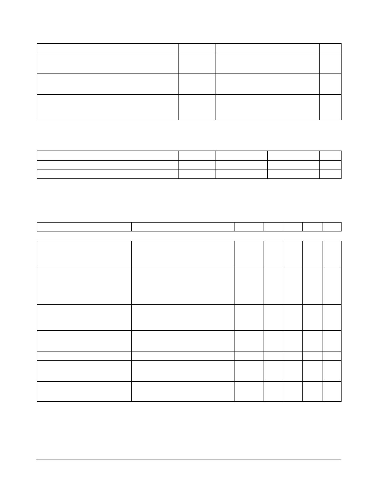
THERMAL CHARACTERISTICS (Note 6)
Rating
Symbol
Value
Thermal Characteristics, SOIC−14 (Note 6)
Thermal Resistance, Junction−to−Air (Note 7)
Thermal Reference, Junction−to−Lead4 (Note 7)
RqJA
RYJL
95
18.2
Thermal Characteristics, SOIC−8 (Note 6)
Thermal Resistance, Junction−to−Air (Note 7)
Thermal Reference, Junction−to−Lead4 (Note 7)
RqJA
RYJL
132
49.2
Thermal Characteristics, SOIC−8 EP (Note 6)
Thermal Resistance, Junction−to−Air (Note 7)
Thermal Reference, Junction−to−Lead4 (Note 7)
Thermal Reference, Junction−to−Pad (Note 7)
RqJA
RYJL4
RYJPad
80
28.5
14.8
6. Refer to ELECTRICAL CHARACTERISTICS and APPLICATION INFORMATION for Safe Operating Area.
7. Values based on copper area of 645 mm2 (or 1 in2) of 1 oz copper thickness and FR4 PCB substrate.
Unit
°C/W
°C/W
°C/W
RECOMMENDED OPERATING RANGES (Note 8)
Rating
Symbol
Min
Max
Unit
Input Voltage (Note 9)
Vin
4.5
40
V
Junction Temperature
TJ
−40
150
°C
8. Refer to ELECTRICAL CHARACTERISTICS and APPLICATION INFORMATION for Safe Operating Area.
9. Minimum Vin = 4.5 V or (Vout + VDO), whichever is higher.
ELECTRICAL CHARACTERISTICS
Vin = 13.2 V, Cin = 0.1 mF, Cout = 2.2 mF, for typical values TJ = 25°C, for min/max values TJ = −40°C to 150°C; unless otherwise noted.
(Notes 10 and 11)
Parameter
Test Conditions
Symbol Min Typ Max Unit
REGULATOR OUTPUT
Output Voltage (Accuracy %)
3.3 V
5.0 V
TJ = 25°C to 125°C
Vin = 4.5 V to 16 V, Iout = 0.1 mA to 100 mA
Vin = 5.5 V to 16 V, Iout = 0.1 mA to 100 mA
Vout
V
3.2505 3.3 3.3495
4.925 5.0 5.075
(−1.5%)
(+1.5%)
Output Voltage (Accuracy %)
3.3 V
5.0 V
Vout
V
Vin = 4.5 V to 40 V, Iout = 0.1 mA to 100 mA
3.234 3.3 3.366
Vin = 4.5 V to 16 V, Iout = 0.1 mA to 150 mA
3.234 3.3 3.366
Vin = 5.55 V to 40 V, Iout = 0.1 mA to 100 mA
4.9 5.0 5.1
Vin = 5.7 V to 16 V, Iout = 0.1 mA to 150 mA
4.9 5.0 5.1
(−2%)
(+2%)
Output Voltage (Accuracy %)
3.3 V
5.0 V
TJ = −40°C to 125°C
Vin = 4.5 V to 28 V, Iout = 0 mA
Vin = 5.5 V to 28 V, Iout = 0 mA
Vout
V
3.234 3.3 3.366
4.9 5.0 5.1
(−2%)
(+2%)
Line Regulation
5.0 V
3.3 V
Vin = 5.5 V to 28 V, Iout = 5 mA
Vin = 4.5 V to 28 V, Iout = 5 mA
Regline
−20
0
20
mV
Load Regulation
Iout = 0.1 mA to 150 mA
Regload
−40
10
40
mV
Dropout Voltage (Note 12)
5.0 V
Iout = 100 mA
Iout = 150 mA
VDO
mV
−
225 450
−
300 600
Output Capacitor for Stability (Note 13)
Iout = 5 mA to 150 mA
Iout = 0 mA to 5 mA
Cout
ESR
2.2
−
−
mF
−
−
100
W
1
−
100
W
10. Refer to ABSOLUTE MAXIMUM RATINGS and APPLICATION INFORMATION for Safe Operating Area.
11. Performance guaranteed over the indicated operating temperature range by design and/or characterization tested at TA [TJ. Low duty
cycle pulse techniques are used during testing to maintain the junction temperature as close to ambient as possible.
12. Measured when output voltage falls 100 mV below the regulated voltage at Vin = 13.2 V. If Vout < 5 V, then VDO = Vin – Vout. Maximum dro-
pout voltage value is limited by minimum input voltage Vin = 4.5 V recommended for guaranteed operation at maximum output current.
13. Values based on design and/or characterization.
14. Recommended for typical trigger time. TWD = tCW + 1/2 * tOW
http://onsemi.com
4
Share Link: 