NCV8668 データシートの表示(PDF) - ON Semiconductor
部品番号
コンポーネント説明
一致するリスト
NCV8668 Datasheet PDF : 21 Pages
| |||
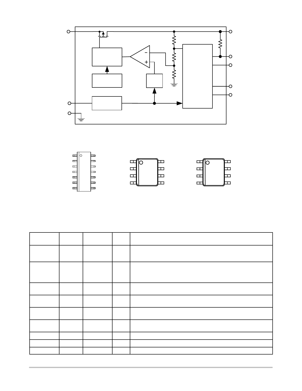
Vin
EN
GND
Driver with
Current
Limit
Thermal
Shutdown
Enable
NCV8668
Vref
Vout
*
RESET
GENERATOR
and
WINDOW
WATCHDOG
RO
WDI
WM1
WM2
* 5 V OPTION ONLY
Figure 2. Simplified Block Diagram
1
RO
GND
GND
GND
GND
WM 2
WM 1
14
EN
Vin
GND
GND
GND
Vout
WDI
SOIC−14
1
RO
GND
WM 2
WM 1
SOIC−8
8
EN
Vin
Vout
WDI
1
RO
GND
WM 2
WM 1
8
EN
Vin
Vout
WDI
SOIC−8 EP
Figure 3. Pin Connections
(Top View)
PIN FUNCTION DESCRIPTION
Pin No.
SOIC−14
Pin No.
SOIC−8
Pin No.
SOIC−8 EP
1
1
1
2, 3, 4, 5, 10,
2
2
11, 12
6
3
3
7
4
4
8
5
5
9
6
6
13
7
7
14
8
8
EPAD
Pin
Name
RO
GND
WM2
WM1
WDI
Vout
Vin
EN
GND
Description
Reset Output. 30 kW internal Pull−Up resistor connected to Vout. (Open Drain
output for 2.5 V, 2.6 V, and 3.3 V voltage options) RO goes Low when Vout
drops by more than 7% from nominal.
Power Supply Ground.
For SOIC−14
− connect pin 2 and 3 to GND
− connect pin 4−5 and 10−12 to heatsink area with GND potential
Watchdog Mode Bit 2; Watchdog and Reset mode selection. Connect to Vout
or GND.
Watchdog Mode Bit 1; Watchdog and Reset mode selection. Connect to Vout
or GND.
Watchdog Input; Trigger Input for Watchdog pulses. When not used, connect
to Vout or GND.
Regulated Output Voltage. Connect 2.2 mF capacitor with ESR < 100 W to
ground.
Positive Power Supply Input. Connect 0.1 mF capacitor to ground.
Enable Input; low level disables the IC.
Exposed Pad is Connected to Ground
http://onsemi.com
2
Share Link: 