NCV8668 データシートの表示(PDF) - ON Semiconductor
部品番号
コンポーネント説明
一致するリスト
NCV8668 Datasheet PDF : 21 Pages
| |||
NCV8668
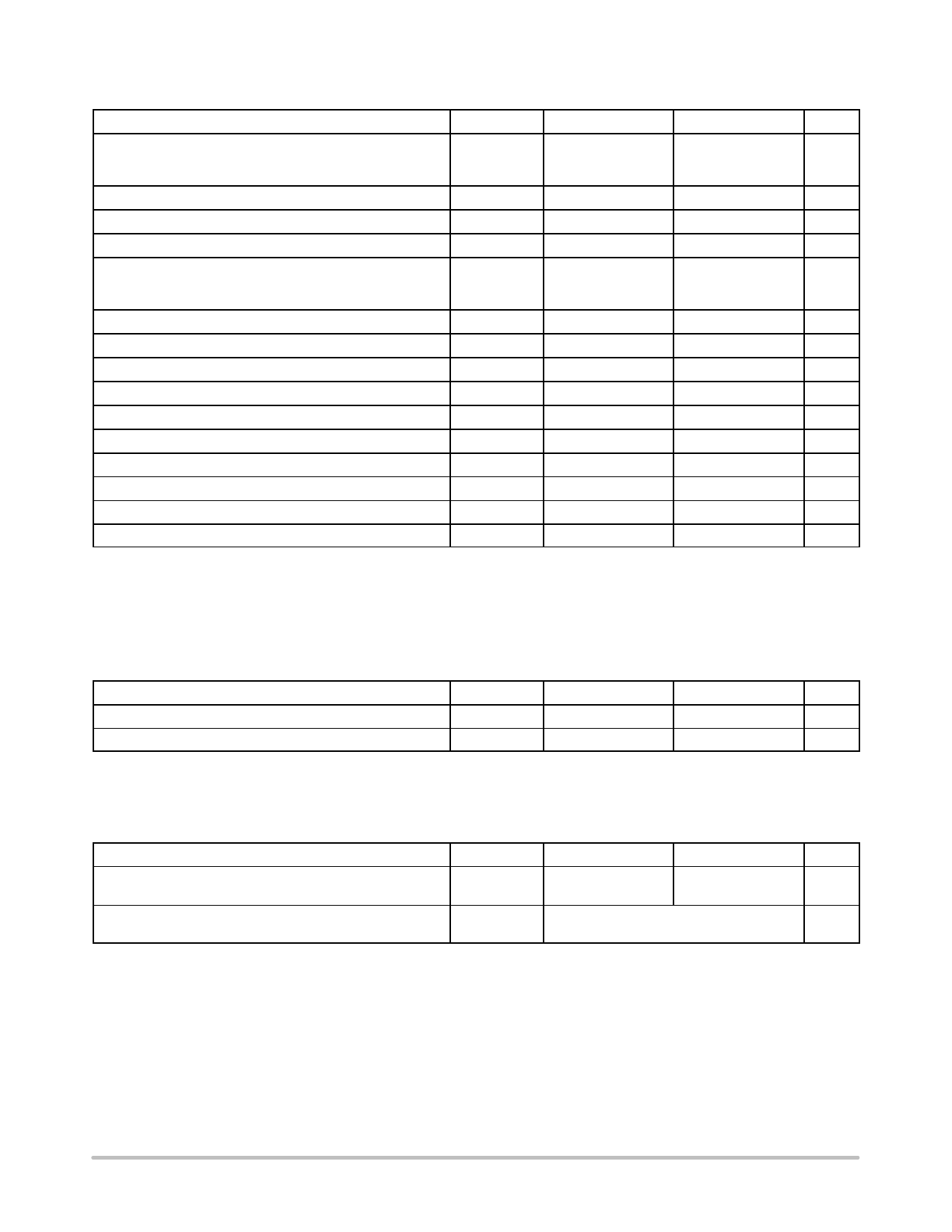
ABSOLUTE MAXIMUM RATINGS
Rating
Symbol
Min
Max
Unit
Input Voltage (Note 1)
DC
Transient, t < 100 ms
Vin
−0.3
−
V
40
45
Input Current
Output Voltage (Note 2)
Output Current
Enable Input Voltage Range
DC
Transient, t < 100 ms
Iin
−5
−
mA
Vout
−0.3
5.5
V
Iout
−3
Current Limited
mA
VEN
−0.3
−
V
40
45
Enable Input Current Range
IEN
−1
1
mA
Reset Output Voltage (Note 3)
VRO
−0.3
5.5
V
Reset Output Current
IRO
−3
3
mA
Watchdog Input Voltage
VWDI
−0.3
5.5
V
Watchdog Mode 1 Voltage
VWM1
−0.3
5.5
V
Watchdog Mode 1 Current
IWM1
−5
5
mA
Watchdog Mode 2 Voltage
VWM2
−0.3
5.5
V
Watchdog Mode 2 Current
IWM2
−5
5
mA
Junction Temperature
TJ
−40
150
°C
Storage Temperature
TSTG
−55
150
°C
Stresses exceeding Maximum Ratings may damage the device. Maximum Ratings are stress ratings only. Functional operation above the
Recommended Operating Conditions is not implied. Extended exposure to stresses above the Recommended Operating Conditions may affect
device reliability.
1. Refer to ELECTRICAL CHARACTERISTICS and APPLICATION INFORMATION for Safe Operating Area.
2. The Output voltage must not exceed the Input voltage.
3. The Reset Output voltage must not exceed the Output voltage.
ESD CAPABILITY (Note 4)
Rating
Symbol
Min
ESD Capability, Human Body Model
ESDHBM
−2
ESD Capability, Machine Model
ESDMM
−200
4. This device series incorporates ESD protection and is tested by the following methods:
ESD Human Body Model tested per AEC−Q100−002 (JS−001−2010)
ESD Machine Model tested per AEC−Q100−003 (EIA/JESD22−A115)
Max
Unit
2
kV
200
V
LEAD SOLDERING TEMPERATURE AND MSL (Note 5)
Rating
Symbol
Min
Max
Unit
Lead Temperature Soldering
TSLD
−
Reflow (SMD Styles Only), Pb−Free Versions (Note 5)
265 peak
°C
Moisture Sensitivity Level
(SOIC−14, SOIC−8)
(SOIC−8EP)
MSL
1
−
2
5. For information, please refer to our Soldering and Mounting Techniques Reference Manual, SOLDERRM/D
http://onsemi.com
3
Share Link: 