NCV8665 データシートの表示(PDF) - ON Semiconductor
部品番号
コンポーネント説明
一致するリスト
NCV8665 Datasheet PDF : 13 Pages
| |||
NCV8665
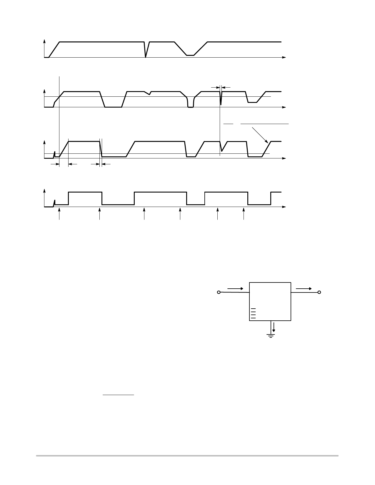
VI
VQ
VD
Reset
Delay Time
VRO
Reset
Reaction
Time
t
< Reset Reaction Time
VQ,rt
t
dVD
dt
+
Reset
Charge
CD
Current
Upper Timing Threshold VDU
Lower Timing Threshold VDL
t
t
Power−on−Reset
Thermal
Shutdown
Voltage Dip
at Input
Undervoltage
Secondary
Spike
Figure 11. Reset Timing
Overload
at Output
Calculating Power Dissipation
in a Single Output Linear Regulator
The maximum power dissipation for a single output
regulator (Figure 12) is:
PD(max) + [VI(max) * VQ(min)] IQ(max)
(1)
) VI(max)Iq
where
VI(max)
voltage,
is the maximum input
VQ(min)
voltage,
is the minimum output
IQ(max)
is the maximum output
current for the application,
Iq is the quiescent current the regulator consumes
at IQ(max).
Once the value of PD(max) is known, the maximum
permissible value of RqJA can be calculated:
RqJA
+
150°
C*
PD
TA
(2)
The value of RqJA can then be compared with those in the
package section of the data sheet. Those packages with
RqJA’s less than the calculated value in Equation NO TAG
will keep the die temperature below 150°C.
In some cases, none of the packages will be sufficient to
dissipate the heat generated by the IC, and an external
heatsink will be required.
II
IQ
VI
SMART
VQ
REGULATOR®
} Control
Features
Iq
Figure 12. Single Output Regulator with Key
Performance Parameters Labeled
Heatsinks
A heatsink effectively increases the surface area of the
package to improve the flow of heat away from the IC and
into the surrounding air.
Each material in the heat flow path between the IC and the
outside environment will have a thermal resistance. Like
series electrical resistances, these resistances are summed to
determine the value of RqJA:
RqJA + RqJC ) RqCS ) RqSA
(3)
http://onsemi.com
8
Share Link: 