NCV8665 データシートの表示(PDF) - ON Semiconductor
部品番号
コンポーネント説明
一致するリスト
NCV8665 Datasheet PDF : 13 Pages
| |||
NCV8665
Linear Regulator - Low
Dropout, Very Low Iq,
Reset, Delay Reset
150 mA
The NCV8665 is a precision 5.0 V fixed output, low dropout
integrated voltage regulator with an output current capability of
150 mA. Careful management of light load current consumption,
combined with a low leakage process, achieve a typical quiescent
ground current of 30 mA.
NCV8665 is pin for pin compatible with the NCV8675 and the
NCV4275 and it could replace this part when lower output current,
and very low quiescent current is required.
The output voltage is accurate within ±2.0%, and maximum dropout
voltage is 600 mV at full rated load current.
It is internally protected against 45 V input transients, input supply
reversal, output overcurrent faults, and excess die temperature. No
external components are required to enable these features.
Features
• 5 V Fixed Output (3.3 V and 2.5 V Versions are Also Available)
• ±2.0% Output Accuracy, Over Full Temperature Range
• 40 mA Maximum Quiescent Current at IOUT = 100 mA
• 600 mV Maximum Dropout Voltage at 150 mA Load Current
• Wide Input Voltage Operating Range of 5.5 V to 45 V
• Internal Fault Protection
♦ −42 V Reverse Voltage
♦ Short Circuit
♦ Thermal Overload
• NCV Prefix for Automotive and Other Applications Requiring Site
and Control Changes
• These are Pb−Free Devices
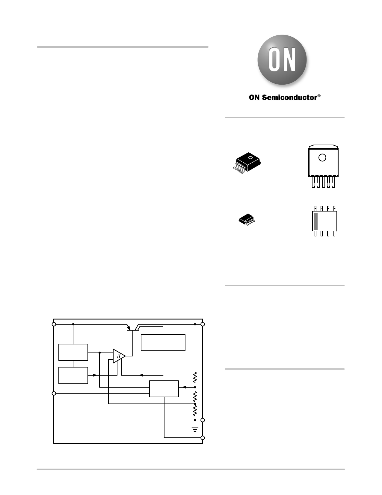
VIN
Bandgap
Reference
Error
Amplifier
+
−
Current Limit and
Saturation Sense
VOUT
http://onsemi.com
MARKING
DIAGRAMS
1
5
D2PAK
5−PIN
DS SUFFIX
CASE 936A
V665−50G
AWLYWWG
1
8
1
SOIC−8
D SUFFIX
CASE 751
8
V6655
ALYWX
G
1
A
= Assembly Location
WL, L = Wafer Lot
Y
= Year
WW, W = Work Week
G or G = Lead Free Indicator
PIN CONNECTIONS
D2PAK
SOIC−8
Pin
1. VIN
Pin
2. RO
Tab,
3. GND*
4. D
5. VOUT
* Tab is connected to Pin 3
1. VIN
2. RO
3. D
4. VOUT
5−8. GND
Thermal
Shutdown
D
Reset
Generator
ORDERING INFORMATION
See detailed ordering and shipping information in the
dimensions section on page 9 of this data sheet.
Figure 1. Block Diagram
© Semiconductor Components Industries, LLC, 2008
October, 2019− Rev. 1
GND
RO
1
Publication Order Number:
NCV8665/D
Share Link: 