NCV8665 データシートの表示(PDF) - ON Semiconductor
部品番号
コンポーネント説明
一致するリスト
NCV8665 Datasheet PDF : 13 Pages
| |||
NCV8665
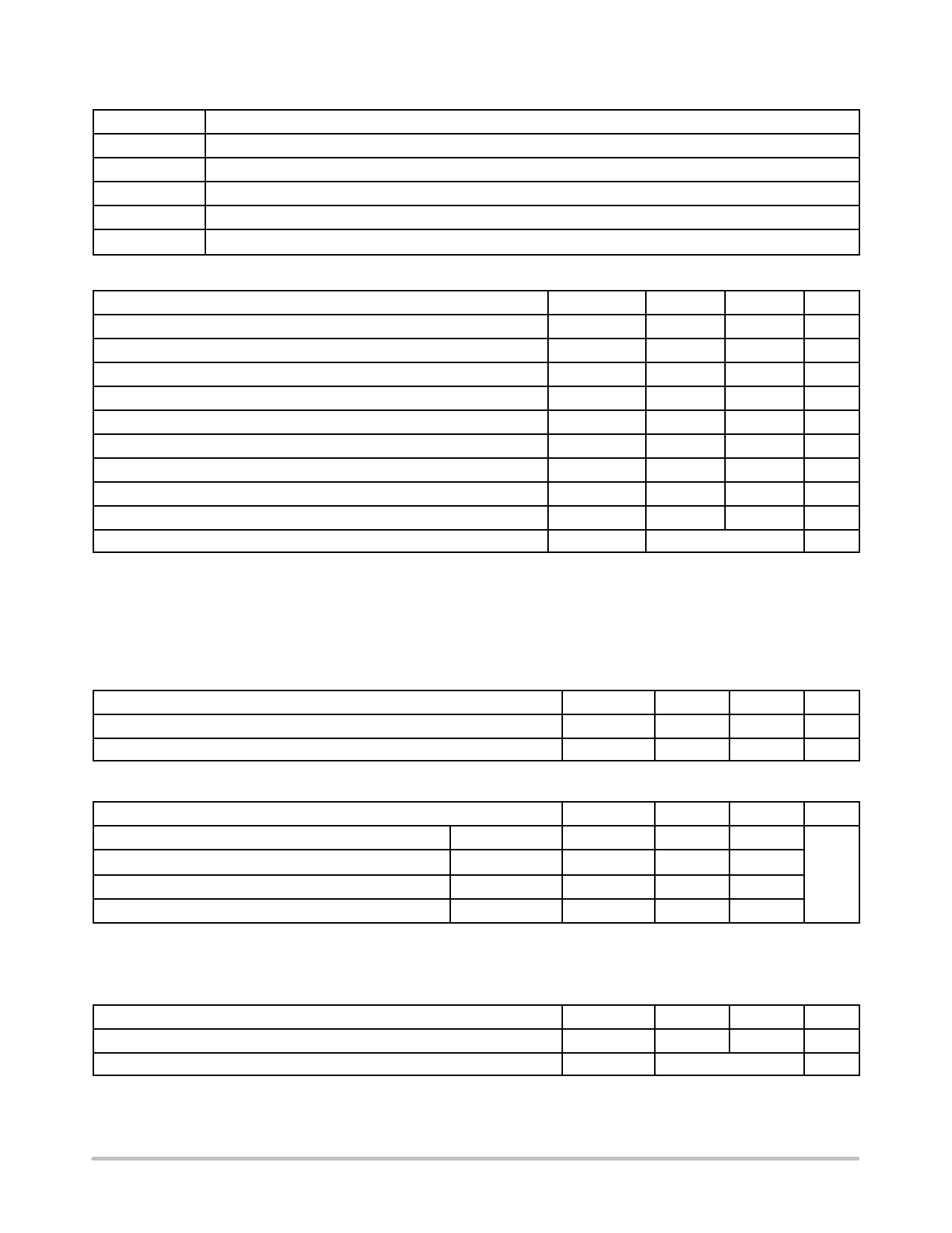
PIN DESCRIPTIONS
Symbol
Function
VIN
RO
GND
Unregulated input voltage; 5.5 V to 45 V; Battery Input Voltage. Bypass to GND with a 0.1 mF ceramic capacitor.
Reset Output; open collector active Reset (Accurate when VOUT > 1.0 V)
Ground; Pin 3 internally connected to Tab
D
Reset Delay; timing capacitor to GND for Reset Delay function
VOUT
Output; ±2.0%, 150 mA. 10 mF, ESR < 16 W
ABSOLUTE MAXIMUM RATINGS
Pin Symbol, Parameter
Symbol
Min
Max
Unit
VIN, DC Input Voltage
VOUT, DC Voltage
Reset Output Voltage
Reset Output Current
Reset Delay Voltage
Reset Delay Current
Storage Temperature
ESD Capability, Human body Model (Note 1)
ESD Capability, Machine Model (Note 1)
Moisture Sensitivity Level
VIN
VOUT
VRO
IRO
VD
ID
TSTG
VESDHB
VESDMM
MSL
−42
+45
V
−0.3
+16
V
−0.3
25
V
−5.0
5.0
mA
−0.3
7.0
V
−2.0
2.0
mA
−55
+150
°C
4000
V
200
V
1
−
Stresses exceeding Maximum Ratings may damage the device. Maximum Ratings are stress ratings only. Functional operation above the
Recommended Operating Conditions is not implied. Extended exposure to stresses above the Recommended Operating Conditions may affect
device reliability.
1. This device series incorporates ESD protection and is tested by the following methods:
ESD Human Body Model (HBM) tested per AEC−Q100−002 (EIA/JESD22−A 114C)
ESD Machine Model (MM) tested per AEC−Q100−003 (EIA/JESD22−A 115C)
2. Latchup Current Maximum Rating: ≤ 100 mA per JEDEC standard: JESD78.
OPERATING RANGE
Pin Symbol, Parameter
Input Voltage Operating Range
Junction Temperature
Symbol
Min
Max
Unit
VIN
5.5
45
V
TJ
−40
150
°C
THERMAL RESISTANCE
Parameter
Symbol
Min
Max
Unit
Junction to Ambient (Note 3)
Junction to Case (Note 3)
Junction to Ambient (Note 4)
D2PAK
D2PAK
SOIC−8
RqJA
RqJC
RqJA
−
85.4
−
6.8
°C/W
−
138
Junction to Lead 6 (Note 4)
SOIC−8
YqJL6
−
21
3. As mounted on a 35x35x1mm FR4 PCB with a single layer of 100 mm2 of 1 oz copper heat spreading area.
4. As mounted on a 35x35x1mm FR4 PCB with a single layer of 100 mm2 of 1 oz copper heat spreading area including traces directly connected
to the leads.
Pb SOLDERING TEMPERATURE AND MSL
Parameter
Lead Temperature Soldering Reflow (SMD styles only), Pb−Free (Note 5)
MSL, 8−Lead EP, LS Temperature 260°C
5. This device series incorporates ESD protection and exceeds the following ratings:
Human Body Model (HBM) v 2.0 kV per JEDEC standard: JESD22–A114.
Machine Model (MM) v 200 V per JEDEC standard: JESD22–A115.
Symbol
Tsld
MSL
Min
Max
Unit
−
265 pk
°C
1
−
http://onsemi.com
2
Share Link: 