MX7824KCAG データシートの表示(PDF) - Maxim Integrated
部品番号
コンポーネント説明
一致するリスト
MX7824KCAG Datasheet PDF : 12 Pages
| |||
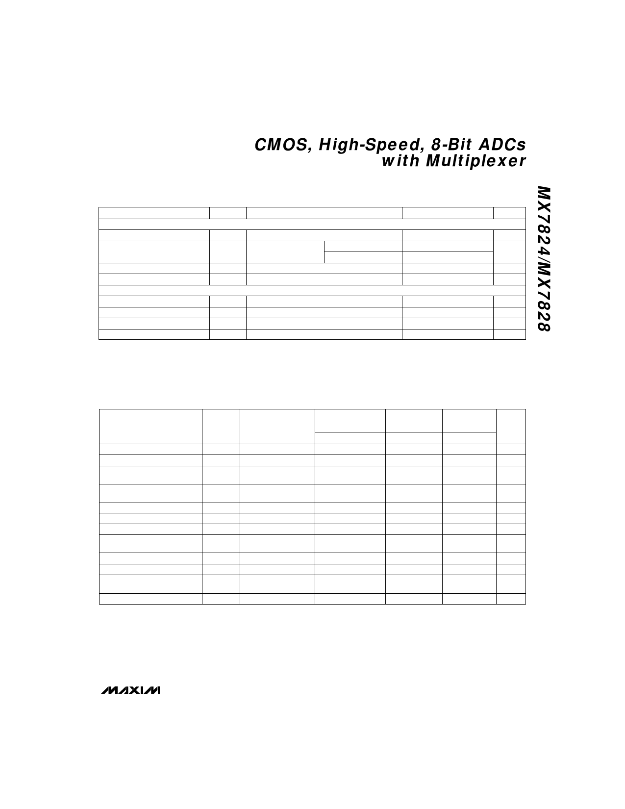
CMOS, High-Speed, 8-Bit ADCs
with Multiplexer
ELECTRICAL CHARACTERISTICS
(VDD = +5V, VREF+ = +5V, VREF- = GND, Mode 0, TA = TMIN to TMAX, unless otherwise noted.)
PARAMETER
LOGIC OUTPUTS
Output High Voltage
Output Low Voltage
Three-State Output Current
Output Capacitance (Note 4)
POWER SUPPLY
Supply Voltage
Supply Current
Power Dissipation
Power-Supply Sensitivity
SYMBOL
CONDITIONS
VOH
VOL
COUT
DB0–DB7,—–IN—T–; IOUT = -360µA
DB0–DB7,—–IN—T–; RDY
IOUT = 1.6mA
IOUT = 2.6mA
DB0–DB7, RDY; VOUT = 0V to VDD
VDD 5V ±5% for specified performance
IDD
–C—S– = –R—D– = 2.4V
PSS VDD = ±5%
MIN TYP MAX UNITS
4.0
V
0.4
V
0.4
±3
µA
5
8
pF
4.75
5.25
V
15
mA
25
75
mW
±1/16 ±1/4 LSB
Note 1: Total unadjusted error includes offset, full-scale, and linearity errors.
Note 2: Specified with no external load unless otherwise noted.
Note 3: Temperature drift is defined as change in output voltage from +25°C to TMIN or TMAX divided by (25 - TMIN) or (TMAX - 25).
Note 4: Guaranteed by design.
TIMING CHARACTERISTICS (Note 5)
(VDD = +5V, VREF+ = +5V, VREF- = GND, Mode 0, TA = TMIN to TMAX, unless otherwise noted.)
PARAMETER
–C—S– to –R—D– Setup Time
–C—S– to –R—D– Hold Time
Multiplexer Address
Setup Time
Multiplexer Address
Hold Time
–C—S– to RDY Delay
Conversion Time (Mode 0)
Data Access Time After R–—D–
DAfatetar—–IAN—cT–c,eMssodTeim0e
–R—D– to—–IN—T– Delay (Mode 1)
Data Hold Time
Delay Time
Between Conversions
–R—D– Pulse Width (Mode 1)
SYMBOL
tCSS
tCSH
tAS
CONDITIONS
TA = +25°C
MAX15_ _C/E
MX782_K/L/B/C
MIN TYP MAX MIN
0
0
0
0
MAX
MAX15_ _M
MX782_T/U
MIN MAX
0
0
UNITS
ns
ns
0
0
0
ns
tAH
30
35
40
ns
tRDY CL = 50pF, RL = 5kΩ
30 40
60
tCRD
1.6 2.0
2.4
tACC1 (Note 6)
85
110
60
ns
2.8
µs
120 ns
tACC2 (Note 6)
20 50
60
70
ns
tINTH
tDH
CL = 50pF
(Note 7)
40 75
100
100 ns
60
70
70
ns
tP
500
500
600
ns
tRD
60
600 80
500
80
400
ns
Note 5: All input control signals are specified with tR = tF = 20ns (10% to 90% of +5V) and timed from a 1.6V voltage level.
Note 6: Measured with load circuits of Figure 1 and defined as the time required for an output to cross 0.8V or 2.4V.
Note 7: Defined as the time required for the data lines to change 0.5V when loaded with the circuits of Figure 2.
_______________________________________________________________________________________ 3
Share Link: 