MSM7731-02 データシートの表示(PDF) - Oki Electric Industry
部品番号
コンポーネント説明
一致するリスト
MSM7731-02 Datasheet PDF : 53 Pages
| |||
1Semiconductor
FEDL7731-02-04
MSM7731-02
PIN FUNCTIONAL DESCRIPTION
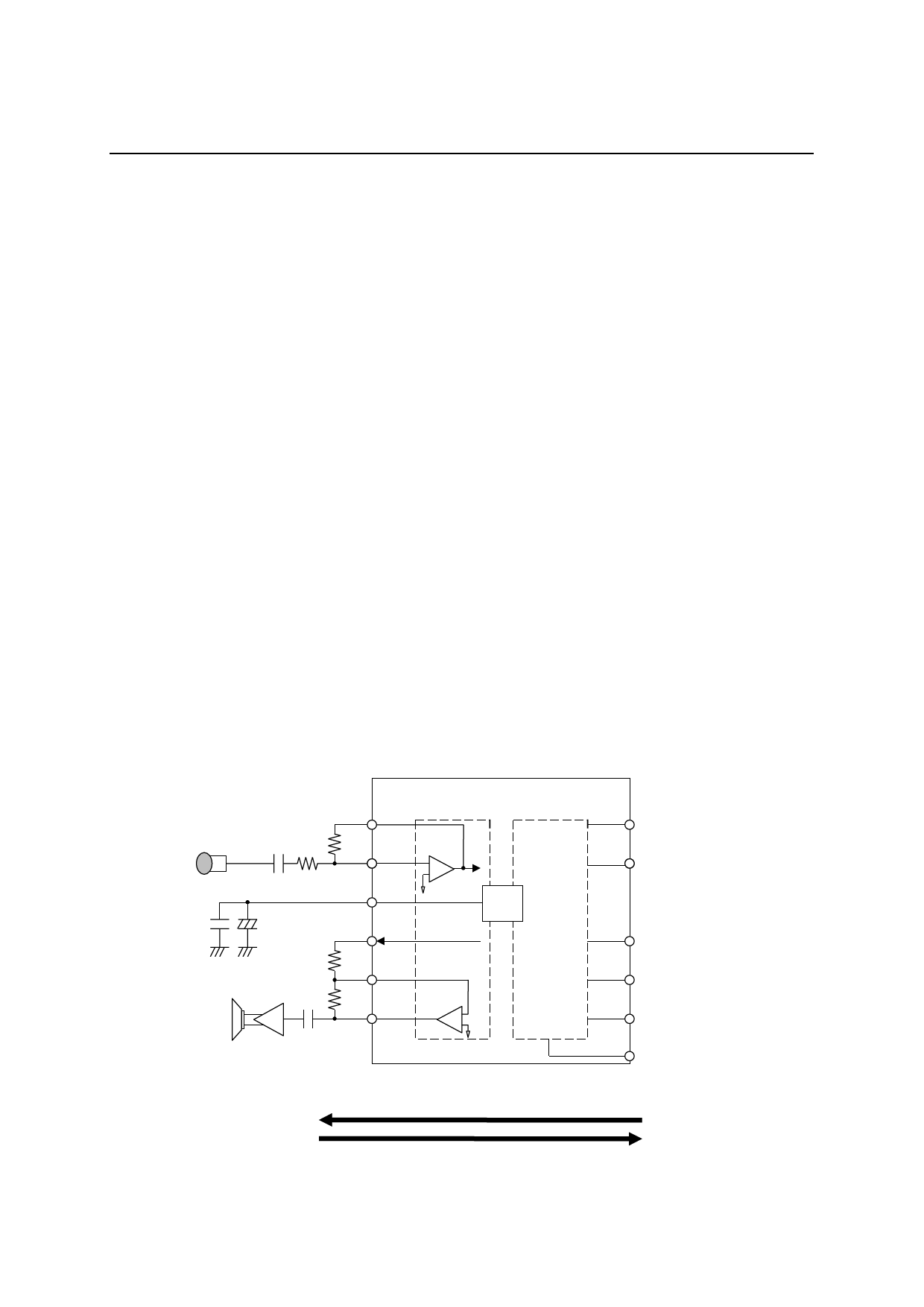
AIN, AGSX
These are the acoustic analog input and level adjusting pins. The AIN pin is connected to the inverting input of the
internal amp and the AGSX pin is connected to the amp output. For level adjustment, refer to the diagram below
(Figure 1). At power-down reset, the AGSX pin goes to a high impedance state.
AVFRO, AOUT, APWI
These are acoustic analog output and level adjusting pins. The AVFRO pin is an audio output and can directly
drive 20 kΩ. The AOUT pin is an analog output and can directly drive a load of 1.2 kΩ. For level adjustment, refer
to the diagram below (Figure 1). At power-down reset, these output pins go to a high impedance state.
LIN, LGSX
These are the line analog input and level adjusting pins. The LIN pin is connected to the inverting input of the
internal amp and the LGSX pin is connected to the amp output. For level adjustment, refer to the diagram below
(Figure 1). At power-down reset, the LGSX pin goes to a high impedance state. If LIN is not used, short the LIN
and LGSX together.
LVFRO, LOUT, LPWI
These are acoustic analog output and level adjusting pins. The LVFRO pin is an audio output and can directly drive
20 kΩ. The LOUT pin is an analog output and can directly drive a load of 1.2 kΩ. For level adjustment, refer to the
diagram below (Figure 1). At power-down reset, these output pins go to a high impedance state. If LOUT is not
used, short the LPWI and LOUT pins together.
LINEEN
This is the power-down control pin for the line CODEC. A logic “0” continues normal operation and a logic “1”
power down only the line CODEC. If the line CODEC is not used, power down the line CODEC and short the LIN
pin to the LGSX pin and the LPWI pin to the LOUT pin. This procedure results in the low consumption of
electrical power. At power-down, the output pins go to a high impedance state. If the pin setting is changed, reset
must be activated by either the PDN/RST pin or the PDN/RST bit (CR0-B7). This pin is ORed with CR0-B5 of the
control register. Refer to the section “RELATIONSHIP BETWEEN PINS AND CONTROL REGISTERS”.
VAGSX/Vi = R2/R1 ≤ 30
VAGSX = 1.3 VPP
R2 ≥ 20 kΩ
MIC Vi
C1 R1
0.1 µF
+
–10 µF
Acoustic CODEC Line CODEC
AGSX
LGSX
R2 AIN
+–
to ENCODER
LIN
SG
VREF
AVFRO
LVFRO
Same as acoustic
analog interface
SPamp
R3 APWI
LPWI
C2 R4
SP
Vo
VO/VAVFRO = R4/R3 ≤ 2
VO = 2.6 VPP,
VAVFRO = 1.3 VPP
R3, R4 ≥ 20 kΩ
Acoustic Side (Mic, Speaker)
AOUT
+–
Receive Signal
Transmit Signal
LOUT
LINEEN
Line Side (Hand Set)
Figure 1 Analog Interface
4/53
Share Link: 