MM74HC32 データシートの表示(PDF) - Fairchild Semiconductor
部品番号
コンポーネント説明
一致するリスト
MM74HC32 Datasheet PDF : 9 Pages
| |||
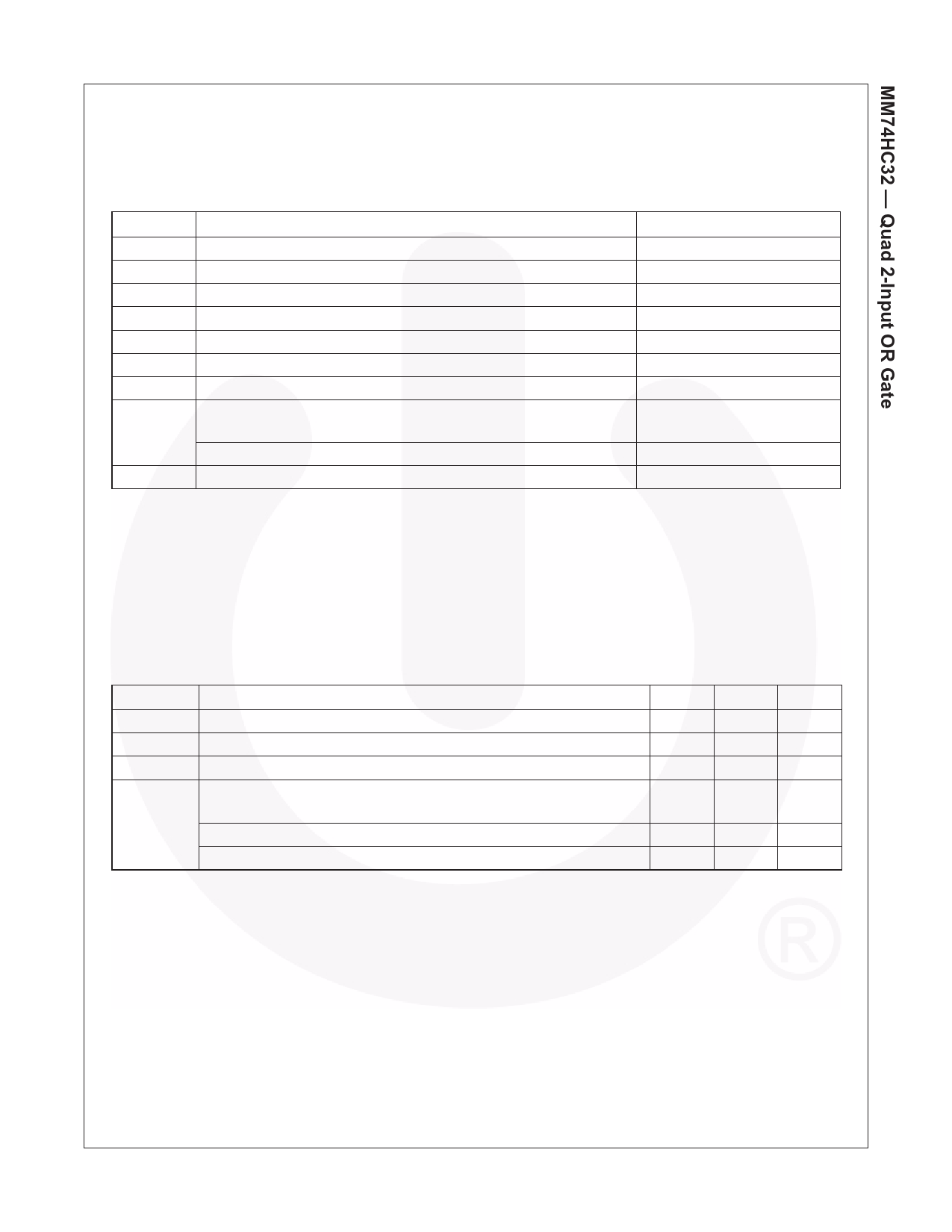
Absolute Maximum Ratings(1)
Stresses exceeding the absolute maximum ratings may damage the device. The device may not function or be
operable above the recommended operating conditions and stressing the parts to these levels is not recommended.
In addition, extended exposure to stresses above the recommended operating conditions may affect device reliability.
The absolute maximum ratings are stress ratings only.
Symbol
Parameter
Rating
VCC
VIN
VOUT
IIK, IOK
IOUT
ICC
TSTG
PD
Supply Voltage
DC Input Voltage
DC Output Voltage
Clamp Diode Current
DC Output Current, per pin
DC VCC or GND Current, per pin
Storage Temperature Range
Power Dissipation
Note 2
–0.5 to +7.0V
–1.5 to VCC+1.5V
–0.5 to VCC+0.5V
±20mA
±25mA
±50mA
–65°C to +150°C
600mW
S.O. Package only
500mW
TL
Lead Temperature (Soldering 10 seconds)
260°C
Notes:
1. Unless otherwise specified all voltages are referenced to ground.
2. Power Dissipation temperature derating — plastic “N” package: –12mW/°C from 65°C to 85°C.
Recommended Operating Conditions
The Recommended Operating Conditions table defines the conditions for actual device operation. Recommended
operating conditions are specified to ensure optimal performance to the datasheet specifications. Fairchild does not
recommend exceeding them or designing to absolute maximum ratings.
Symbol
VCC
VIN, VOUT
TA
tr, tf
Parameter
Supply Voltage
DC Input or Output Voltage
Operating Temperature Range
Input Rise or Fall Times
VCC = 2.0V
VCC = 4.5V
VCC = 6.0V
Min.
2
0
–40
Max.
6
VCC
+85
Units
V
V
°C
1000
ns
500
ns
400
ns
©1983 Fairchild Semiconductor Corporation
MM74HC32 Rev. 1.3.0
2
www.fairchildsemi.com
Share Link: 