MCP2140 データシートの表示(PDF) - Microchip Technology
部品番号
コンポーネント説明
一致するリスト
MCP2140
Microchip Technology

MCP2140 Datasheet PDF : 58 Pages
| |||
MCP2140
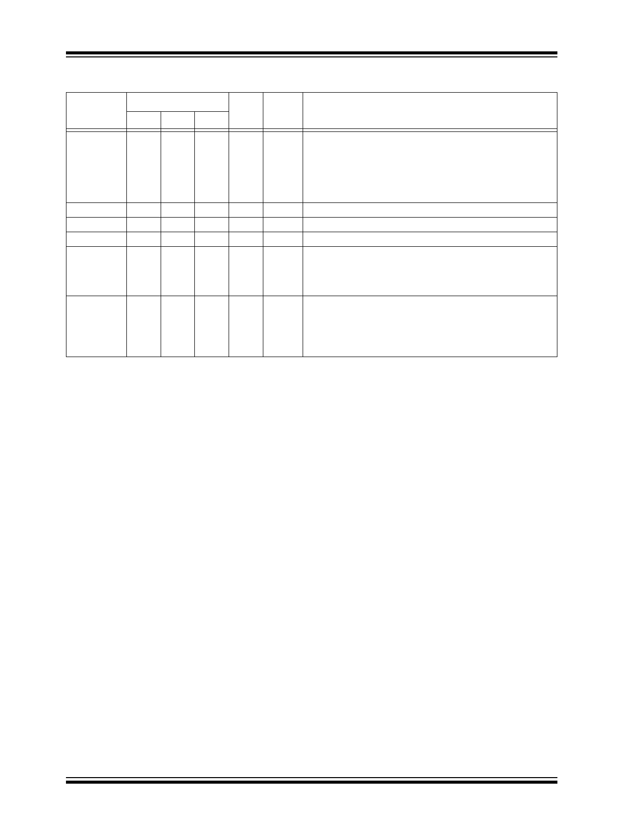
TABLE 1-2: MCP2140 PIN DESCRIPTION NORMAL OPERATION (DCE) (CONTINUED)
Pin Name
Pin Number
Pin Buffer
PDIP SOIC SSOP Type Type
Description
RTS
13 13 14
I
VDD
14
OSC2
15
OSC1/CLKIN 16
CD
17
14 15, 16 —
15 17
O
16 18
I
17 19
I
RXPD
18 18 20
I
Legend:
TTL = TTL compatible input
A = Analog
CMOS = CMOS compatible input
I = Input
TTL Request to Send. Indicates that a Host Controller is ready to
receive data from the MCP2140. This signal is locally emu-
lated and not related to the CTS/RTS bit of the IrDA Primary
device.
1 = Host Controller not ready to receive data
0 = Host Controller ready to receive data
P Positive supply for logic and I/O pins.
— Oscillator crystal output.
CMOS Oscillator crystal input/external clock source input.
ST Carrier Detect. The state of this bit is communicated to the
IrDA Primary device via the IrDA CD bit.
1 = No Carrier Present
0 = Carrier Present
A IR RX Photo Detect Diode input. This input signal is required
to be a pulse to indicate an IR bit. When the amplitude of the
signal crosses the amplitude threshold set by the RXPDREF
pin, the IR bit is detected. The pulse has minimum and max-
imum requirements as specified in Parameter IR131A.
ST = Schmitt Trigger input with CMOS levels
P = Power
OC = Open collector output
O = Output
1: The state of the DTR output pin does not reflect the state of the DTR bit of the IrDA Primary Device.
DS21790A-page 6
Preliminary
2003 Microchip Technology Inc.
Share Link: