M312L2828ET0 データシートの表示(PDF) - Samsung
部品番号
コンポーネント説明
一致するリスト
M312L2828ET0 Datasheet PDF : 23 Pages
| |||
256MB, 512MB, 1GB Registered DIMM
DDR SDRAM
AC Operating Conditions
Parameter/Condition
Input High (Logic 1) Voltage, DQ, DQS and DM signals
Input Low (Logic 0) Voltage, DQ, DQS and DM signals.
Input Differential Voltage, CK and CK inputs
Input Crossing Point Voltage, CK and CK inputs
Symbol
Min
Max
Unit
VIH(AC) VREF + 0.31
V
VIL(AC)
VREF - 0.31
V
VID(AC)
0.7
VDDQ+0.6
V
VIX(AC) 0.5*VDDQ-0.2 0.5*VDDQ+0.2
V
Note
3
3
1
2
Note : 1. VID is the magnitude of the difference between the input level on CK and the input on CK.
2. The value of VIX is expected to equal 0.5*VDDQ of the transmitting device and must track variations in the DC level of the same.
3. These parameters should be tested at the pim on actual components and may be checked at either the pin or the pad in
simulation. the AC and DC input specificatims are refation to a Vref envelope that has been bandwidth limited 20MHz.
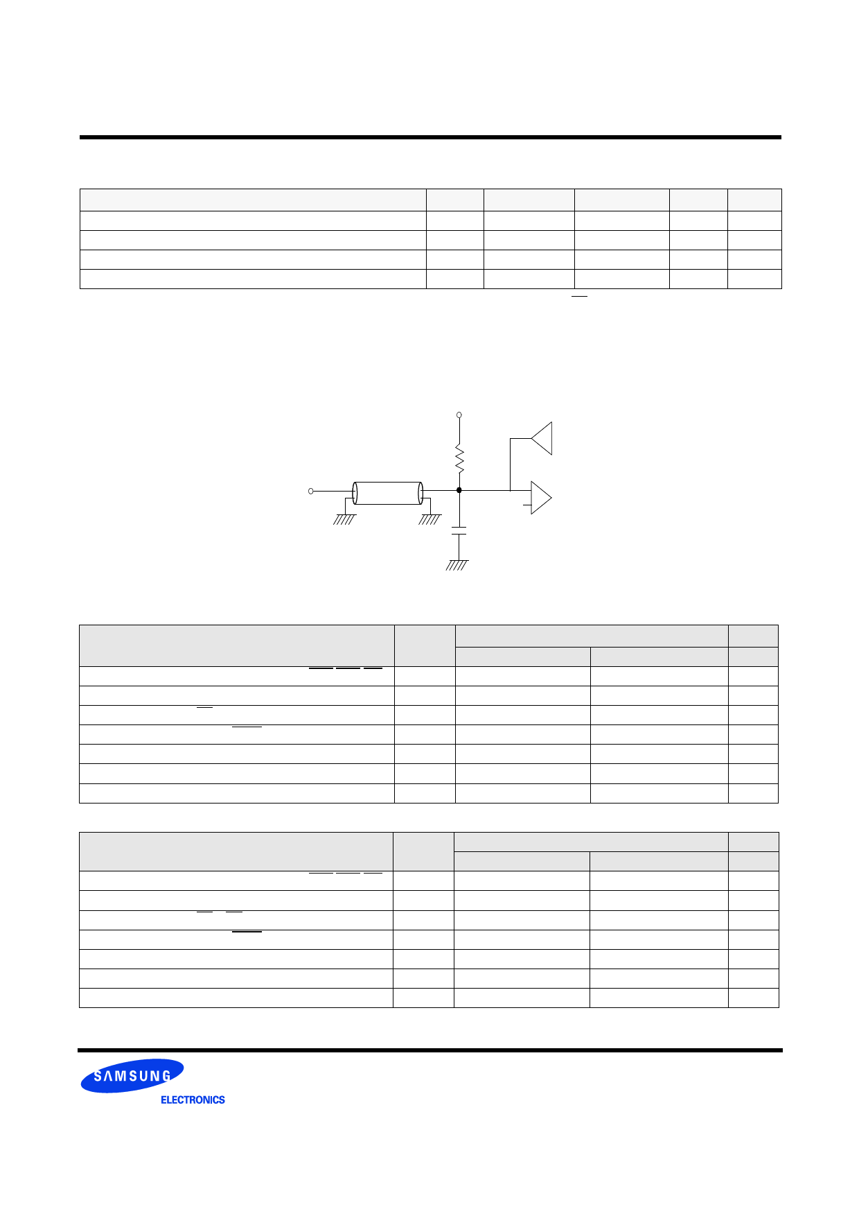
Vtt=0.5*VDDQ
Output
RT=50Ω
Z0=50Ω
CLOAD=30pF
VREF
=0.5*VDDQ
Input/Output Capacitance
Output Load Circuit (SSTL_2)
(VDD=2.5V, VDDQ=2.5V, TA= 25°C, f=1MHz)
Parameter
M383(12)L3223ETS, M383(12)L6420ETS
Unit
Symbol
Min
Max
Input capacitance(A0 ~ A12, BA0 ~ BA1,RAS,CAS,WE ) CIN1
9
Input capacitance(CKE0)
CIN2
9
Input capacitance( CS0)
CIN3
9
11
pF
11
pF
11
pF
Input capacitance( CLK0, CLK0 )
CIN4
11
Input capacitance(DM0~DM8)
CIN5
10
Data & DQS input/output capacitance(DQ0~DQ63)
Cout1
10
12
pF
11
pF
11
pF
Data input/output capacitance (CB0~CB7)
Cout2
10
11
pF
Parameter
M383(12)L6423ETS, M383(12)L2828ET1(0)
Unit
Symbol
Min
Max
Input capacitance(A0 ~ A12, BA0 ~ BA1,RAS,CAS,WE ) CIN1
9
11
pF
Input capacitance(CKE0,CKE1)
CIN2
9
11
pF
Input capacitance( CS0, CS1)
CIN3
9
11
pF
Input capacitance( CLK0, CLK0 )
CIN4
11
12
pF
Input capacitance(DM0~DM8)
CIN5
14
16
pF
Data & DQS input/output capacitance(DQ0~DQ63)
Cout1
14
16
pF
Data input/output capacitance (CB0~CB7)
Cout2
14
16
pF
Revision 1.4 February, 2004
Share Link: 