HFA3861A データシートの表示(PDF) - Intersil
部品番号
コンポーネント説明
一致するリスト
HFA3861A Datasheet PDF : 37 Pages
| |||
HFA3861A
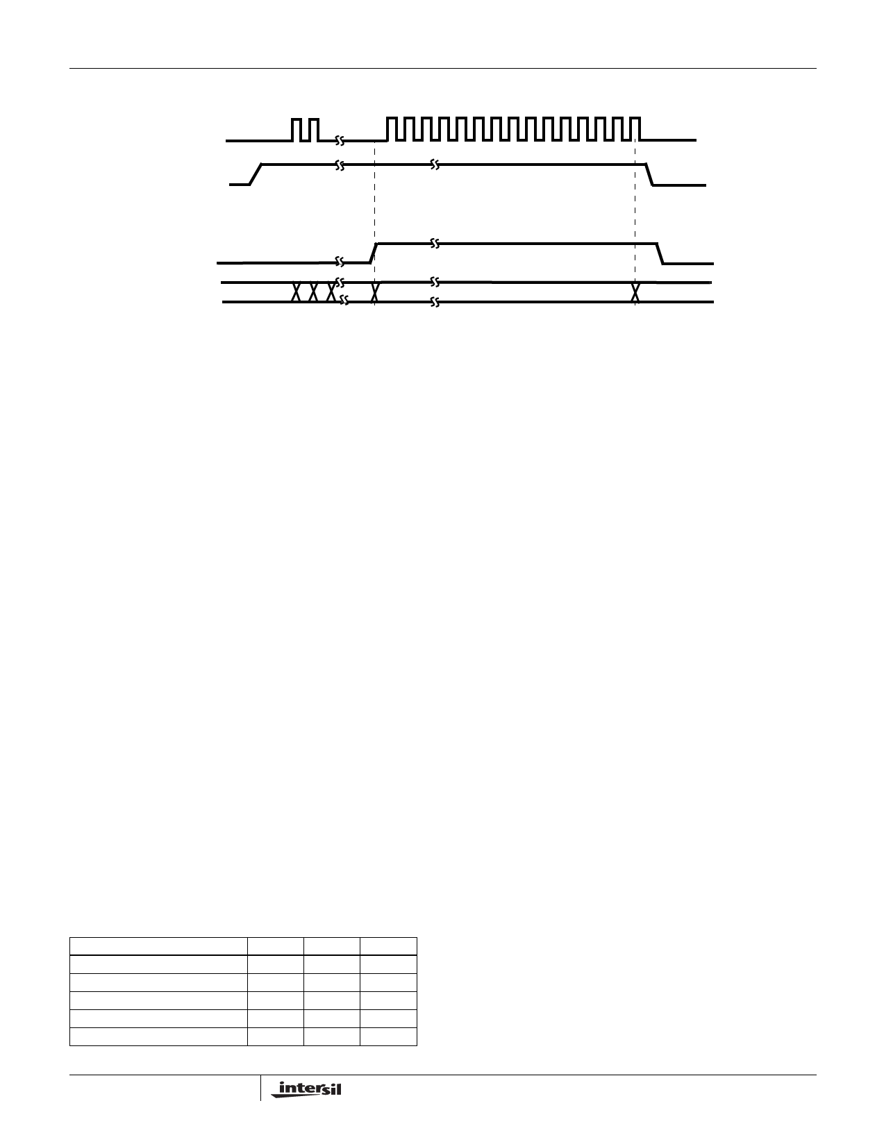
RXCLK
RX_PE
MD_RDY
HEADER
FIELDS
PROCESSING
PREAMBLE/HEADER
DATA
RXD
LSB
DATA PACKET
MSB
NOTE: MD_RDY active after CRC16. See detailed timing diagrams (Figures 18, 19, 20).
FIGURE 5. RX PORT TIMING
RXCLK is an output from the HFA3861A and is the clock
for the serial demodulated data on RXD. MD_RDY is an
output from the HFA3861A and it may be set to go active
after the SFD or CRC fields. Note that RXCLK becomes
active after the Start Frame Delimiter (SFD) to clock out the
Signal, Service, and Length fields, then goes inactive
during the header CRC field. RXCLK becomes active again
for the data. MD_RDY returns to its inactive state after
RX_PE is deactivated by the external controller, or if a
header error is detected. A header error is either a failure of
the CRC check, or the failure of the received signal field to
match one of the 4 programmed signal fields. For either
type of header error, the HFA3861A will reset itself after
reception of the CRC field. If MD_RDY had been set to go
active after CRC, it will remain low.
MD_RDY and RXCLK can be configured through CR 1, bits
1 and 0 to be active low, or active high. The receive port is
completely independent from the operation of the other
interface ports including the TX port, supporting therefore a
full duplex mode.
RX I/Q A/D Interface
The PRISM baseband processor chip (HFA3861A) includes
two 6-bit Analog to Digital converters (A/Ds) that sample the
balanced differential analog input from the IF down
converter. The I/Q A/D clock, samples at twice the chip rate.
The nominal sampling rate is 22MHz.
The interface specifications for the I and Q A/Ds are listed in
Table 1. The HFA3861A is designed to be DC coupled to the
HFA3783.
TABLE 1. I, Q, A/D SPECIFICATIONS
PARAMETER
Full Scale Input Voltage (VP-P)
Input Bandwidth (-0.5dB)
Input Capacitance (pF)
Input Impedance (DC)
fS (Sampling Frequency)
MIN
TYP
MAX
0.90
1.00
1.10
-
11MHz
-
-
2
-
5kΩ
-
-
-
22MHz
-
The voltages applied to pin 16, VREF and pin 21, IREF set
the references for the internal I and Q A/D converters. In
addition, For a nominal I/Q input of 250mVP-P , the
suggested VREF voltage is 1.2V.
AGC Circuit
The AGC circuit is designed to optimize A/D performance for
the I and Q inputs by maintaining the proper headroom on
the 6-bit converters. There are two gain stages being
controlled. At RF, the gain control is a 30dB step in gain from
turning off the LNA. This RF gain control optimizes the
receiver dynamic range when the signal level is high and
maintains the noise figure of the receiver when it is needed
most. At IF the gain control is linear and covers the bulk of
the gain control range of the receiver.
The AGC sensing mechanism uses a combination of the
I and Q A/D converters and the detected signal level in the
IF to determine the gain settings. The A/D outputs are
monitored in the HFA3861A for the desired nominal level.
When it is reached, by adjusting the receiver gain, the gain
control is locked for the remainder of the packet.
RX_AGC_IN Interface
The signal level in the IF stage is monitored to determine
when to impose the up to 30dB gain reduction in the RF
stage. This maximizes the dynamic range of the receiver by
keeping the RF stages out of saturation at high signal levels.
When the IF circuits’ sensor output reaches 0.5V, the
HFA3861A comparator switches in the 30dB pad and
compensates the IF AGC and RSSI measures.
TX I/Q DAC Interface
The transmit section outputs balanced differential analog
signals from the transmit DACs to the HFA3783. These are
DC coupled and digitally filtered.
7
Share Link: 