HFA3861A データシートの表示(PDF) - Intersil
部品番号
コンポーネント説明
一致するリスト
HFA3861A Datasheet PDF : 37 Pages
| |||
HFA3861A
ANALOG
INPUTS
A/D
REFERENCE
POWER
DOWN
SIGNALS
TEST
PORT
ANT_SEL
HFA3861A
RXI
RXQ
AGC
AGC
TXI
TXQ
VREF
IREF
TX_PE
RX_PE
RESET
8
TEST
TXD
TXCLK
TX_RDY
RXD
RXC
MD_RDY
CS
SD
SCLK
R/W
SDI
ANALOG
OUTPUTS
TX_PORT
RX_PORT
CONTROL_PORT
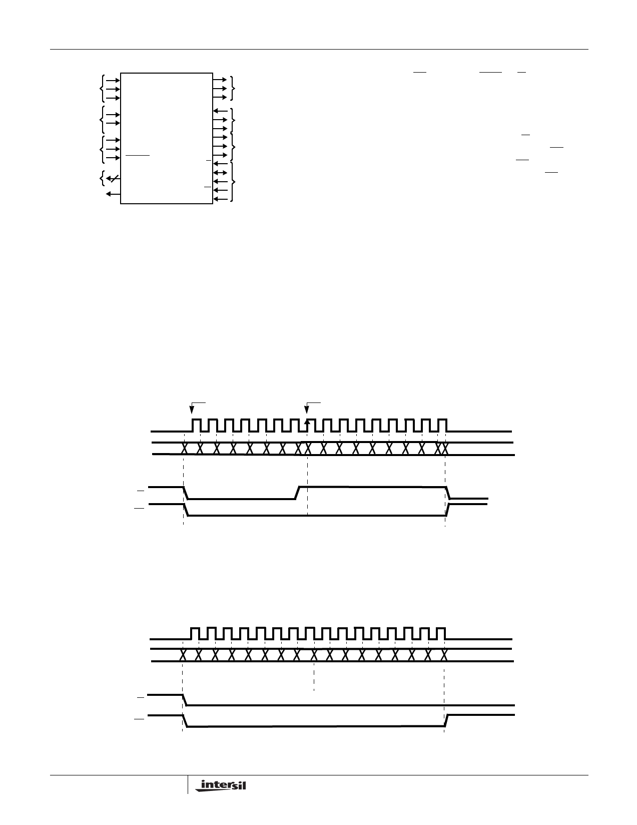
FIGURE 1. EXTERNAL INTERFACES
Control Port (4 Wire)
The serial control port is used to serially write and read
data to/from the device. This serial port can operate up to a
11MHz rate or 1/2 the maximum master clock rate of the
device, MCLK (whichever is lower). MCLK must be running
and RESET must be inactive during programming. This
port is used to program and to read all internal registers.
The first 8 bits always represent the address followed
immediately by the 8 data bits for that register. The LSB of
the address is a don’t care, but reserved for future
expansion. The serial transfers are accomplished through
the serial data pin (SD). SD is a bidirectional serial data
bus. Chip Select (CS), and Read/Write (R/W) are also
required as handshake signals for this port. The clock used
in conjunction with the address and data on SD is SCLK.
This clock is provided by the external source and it is an
input to the HFA3861A. The timing relationships of these
signals are illustrated in Figures 2 and 3. R/W is high when
data is to be read, and low when it is to be written. CS is an
asynchronous reset to the state machine. CS must be
active (low) during the entire data transfer cycle. CS
selects the serial control port device only. The serial control
port operates asynchronously from the TX and RX ports
and it can accomplish data transfers independent of the
activity at the other digital or analog ports.
The HFA3861A has 96 internal registers that can be
configured through the control port. These registers are
listed in the Configuration and Control Internal Register
table. Table 9 lists the configuration register number, a
brief name describing the register, the HEX address to
access each of the registers and typical values. The type
indicates whether the corresponding register is Read only
(R) or Read/Write (R/W). Some registers are two bytes
wide as indicated on the table (high and low bytes).
SCLK
SD
FIRST ADDRESS BIT
FIRST DATABIT OUT
7 6 5 4 3 2 1 07 6 5 4 3 2 1 0
7654321
MSB
ADDRESS IN
76
MSB
54 32
DATA OUT
10
LSB
R/W
CS
NOTES:
1. The HFA3861A always uses the rising edge of SCLK to sample address and data and to generate read data.
2. These figures show the controller using the falling edge of SCLK to generate address and data and to sample read data.
FIGURE 2. CONTROL PORT READ TIMING
SCLK
SD
R/W
CS
7654321076543210
76 5 4 3 2 1 0 7 65 4 3 2 1 0
MSB
ADDRESS IN
MSB
DATA IN
LSB
FIGURE 3. CONTROL PORT WRITE TIMING
5
Share Link: 