HFA3861A データシートの表示(PDF) - Intersil
部品番号
コンポーネント説明
一致するリスト
HFA3861A Datasheet PDF : 37 Pages
| |||
HFA3861A
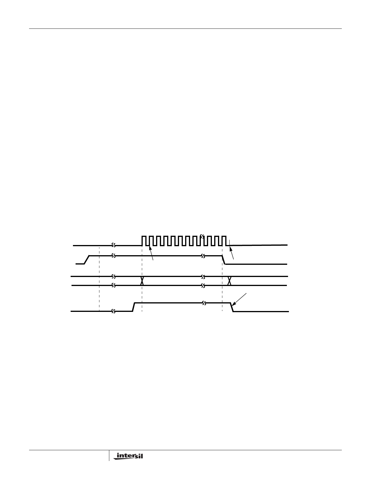
TX Port
The transmit data port accepts the data that needs to be
transmitted serially from an external data source. The data is
modulated and transmitted as soon as it is received from the
external data source. The serial data is input to the
HFA3861A through TXD using the next rising edge of TXCLK
to clock it in the HFA3861A. TXCLK is an output from the
HFA3861A. A timing scenario of the transmit signal
handshakes and sequence is shown on timing diagram Figure
4.
The external processor initiates the transmit sequence by
asserting TX_PE. TX_PE envelopes the transmit data packet
on TXD. The HFA3861A responds by generating a Preamble
and Header. Before the last bit of the Header is sent, the
HFA3861A begins generating TXCLK to input the serial data
on TXD. TXCLK will run until TX_PE goes back to its inactive
state indicating the end of the data packet. The user needs to
hold TX_PE high for as many clocks as there bits to transmit.
For the higher data rates, this will be in multiples of the
number of bits per symbol. The HFA3861A will continue to
output modulated signal for 4µs after the last data bit is output,
to supply bits to flush the modulation path. TX_PE must be
held until the last data bit is output from the MAC/FIFO. The
minimum TX_PE inactive pulse required to restart the
preamble and header generation is 2.22µs and to reset the
modulator is 4.22µs.
The HFA3861A internally generates the preamble and header
information from information supplied via the control registers.
The external source needs to provide only the data portion of
the packet and set the control registers. The timing diagram of
this process is illustrated on Figure 4. Assertion of TX_PE will
initialize the generation of the preamble and header.
TX_RDY, which is an output from the HFA3861A, is used (if
needed) to indicate to the external processor that the
preamble has been generated and the device is ready to
receive the data packet (MPDU) to be transmitted from the
external processor. Signals TX_RDY, TX_PE and TXCLK can
be set individually, by programming Configuration Register
(CR) 1, as either active high or active low signals.
The transmit port is completely independent from the
operation of the other interface ports including the RX port,
therefore supporting a full duplex mode.
RX Port
The timing diagram Figure 5 illustrates the relationships
between the various signals of the RX port. The receive data
port serially outputs the demodulated data from RXD. The
data is output as soon as it is demodulated by the HFA3861A.
RX_PE must be at its active state throughout the receive
operation. When RX_PE is inactive the device's receive
functions, including acquisition, will be in a stand by mode.
TXCLK
TX_PE
FIRST DATA BIT SAMPLED
LAST DATA BIT SAMPLED
TXD
TX_RDY
LSB DATA PACKET
MSB
DEASSERTED WHEN LAST
CHIP OF MPDU CLEARS
MOD PATH OF 3861 EXCEPT FOR
TX FILTER AND D/A
NOTE: Preamble/Header and Data is transmitted LSB first. TXD shown generated from rising edge of TXCLK.
FIGURE 4. TX PORT TIMING
6
Share Link: 