AN-6920MR データシートの表示(PDF) - Fairchild Semiconductor
部品番号
コンポーネント説明
一致するリスト
AN-6920MR
Fairchild Semiconductor

AN-6920MR Datasheet PDF : 17 Pages
| |||
AN-6920
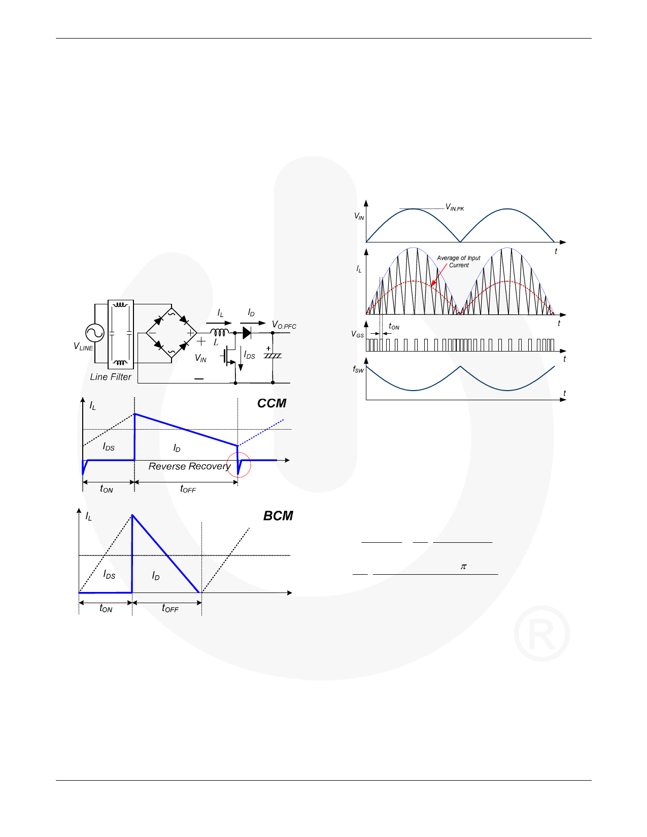
2. Operation Principles of BCM
Boost PFC Converters
The most widely used operation modes for the boost
converter are continuous conduction mode (CCM) and
boundary conduction mode (BCM). These refer to the
current flowing through the energy storage inductor of the
boost converter, as depicted in Figure 2. As the names
indicate, the inductor current in CCM is continuous; while
in BCM, the new switching period is initiated when the
inductor current returns to zero, which is at the boundary of
continuous conduction and discontinuous conduction
operations. Even though the BCM operation has higher
RMS current in the inductor and switching devices, it allows
better switching condition for the MOSFET and the diode.
As shown in Figure 2, the diode reverse recovery is
eliminated and a fast silicon carbide (SiC) diode is not
needed. MOSFET is also turned on with zero current, which
reduces switching loss.
APPLICATION NOTE
source. This behavior makes the boost converter in BCM
operation an ideal candidate for power factor correction.
A by-product of the BCM is that the boost converter runs
with variable switching frequency that depends primarily on
the selected output voltage, the instantaneous value of the
input voltage, the boost inductor value, and the output
power delivered to the load. The operating frequency
changes as the input current follows the sinusoidal input
voltage waveform, as shown in Figure 3. The lowest
frequency occurs at the peak of sinusoidal line voltage.
Figure 2. CCM vs. BCM Control
The fundamental idea of BCM PFC is that the inductor
current starts from zero in each switching period, as shown
in Figure 3. When the power transistor of the boost
converter is turned on for a fixed time, the peak inductor
current is proportional to the input voltage. Since the current
waveform is triangular, the average value in each switching
period is also proportional to the input voltage. In the case
of a sinusoidal input voltage, the input current of the
converter follows the input voltage waveform with a very
high accuracy and draws a sinusoidal input current from the
Figure 3. Operation Waveforms of BCM PFC
The voltage-second balance equation for the inductor is:
VIN (t) ⋅ tON = (VO.PFC −VIN (t)) ⋅ tOFF
(1)
where VIN(t) is the rectified line voltage.
The switching frequency of BCM boost PFC converter is
obtained as:
f SW
1
=
tON + tOFF
1
=
tON
⋅ VO.PFC −VIN (t)
VOUT
= 1 ⋅ VO.PFC −VIN ,PK ⋅ | sin(2π fLINEt) |
(2)
tON
VO.PFC
where VIN,PK is the amplitude of the line voltage and fLINE is
the line frequency.
Figure 4 shows how the MOSFET on time and switching
frequency change as output power decreases. When the load
decreases, as shown in the right side of Figure 4, the peak
inductor current diminishes with reduced MOSFET on time
and the switching frequency increases.
© 2010 Fairchild Semiconductor Corporation
Rev. 1.0.0 • March 10, 2011
2
www.fairchildsemi.com
Share Link: