EM78P569 データシートの表示(PDF) - ELAN Microelectronics
部品番号
コンポーネント説明
一致するリスト
EM78P569 Datasheet PDF : 58 Pages
| |||
User Application Note
(Before using this chip, take a look at the following description note, it includes important messages.)
1. There are some undefined bits in the registers. The values in these bits are unpredicted. These
bits are not allowed to use. We use the symbol “-” in the spec to recognize them.
2. You will see some names for the register bits definitions. Some name will be appear very
frequently in the whole spec. The following describes the meaning for the register’s definitions
such as bit type, bit name, bit number and so on.
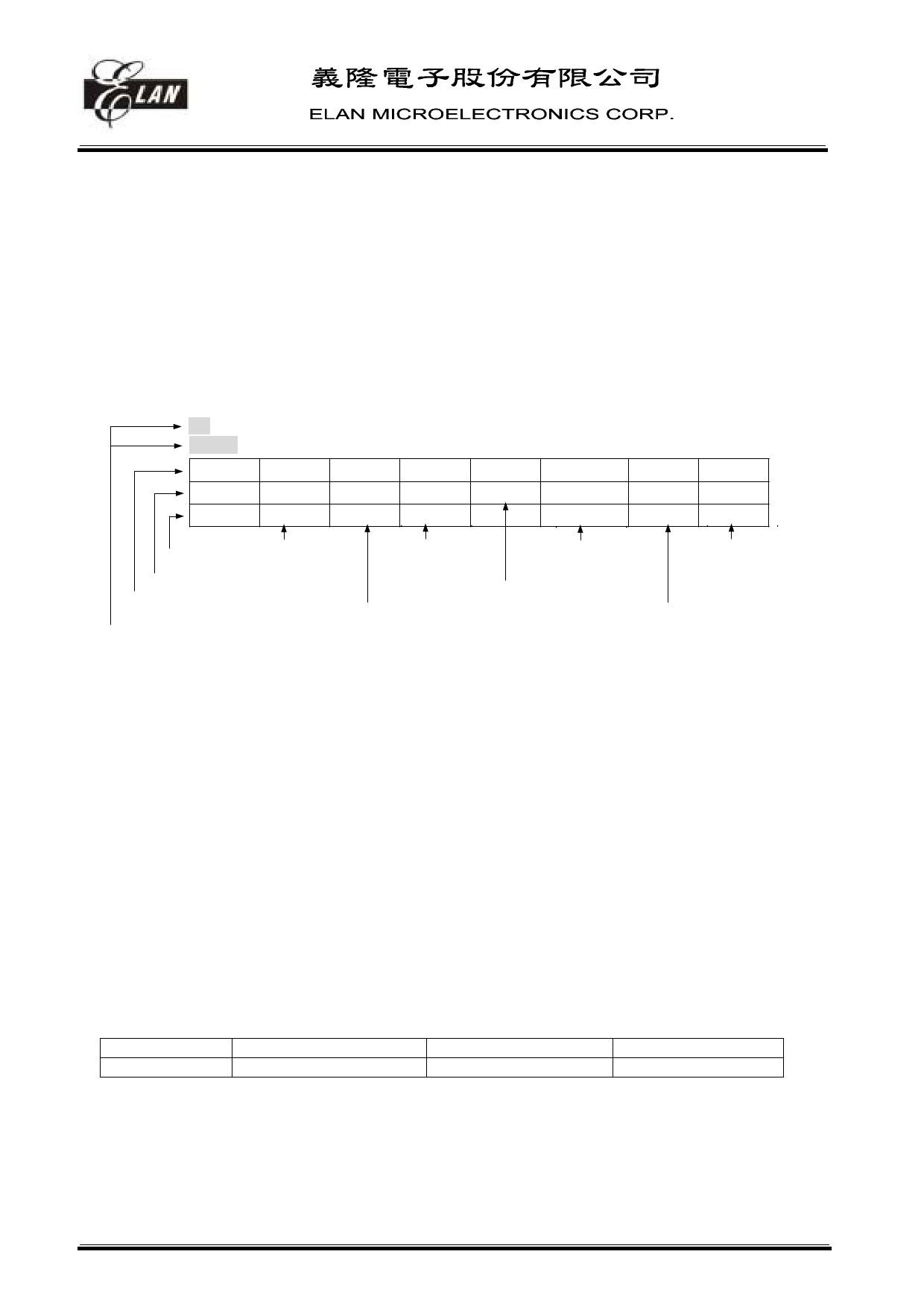
RA
PAGE0
7
6
5
4
3
RAB7 RAB6 BAB5 RAB4
-
R/W-0 R/W-0
R-1
R/W -1
2
RAB2
R
1
RAB1
R-0
0
RAB0
R/W
Bit type
read/write
(default value=0)
read/write
(default value=1)
read only
(w/o default value)
read/write
(w/o default value)
Bit name
Bit number
Register name and its page
read only
(default value=1)
(undefined) not allowed to use
read only
(default value=0)
3. Always set IOCC PAGE1 bit 1 = 1 otherwise partial ADC function cannot be used.
4. For 8 bits resolution DAC, DAO pin will output corresponding voltage after write new data to DAC data buffer(RA
PAGE1). For 10 bits resolution, DAO pin will output constant after change DAC most significant 2 bits (R5 PAGE1
bit6~7). DAO will output correct voltage after write data to least significant 8 bits. That is to say, when using 10 bits
resolution DAC, user must write most significant 2 bits and least significant 8 bits in order.
5. Base on “VERSEL”(code option) equal 0 or 1, R8 page1 and RB page2’s define are different.
“VERSEL” = 0: R8 page1 defined to data RAM address buffer
RB page2 defined to multiplier’s Y data or Y address buffer (controlled by RA page2 bit5 “INDR”).
RA page2 bit4(PLUS) determine RAM address auto increase or not (only for multiplier’s addressing).
RA page2 bit7 is undefined.
“VERSEL” = 1: R8 page1 is undefined.
RA page2 bit4(PLUS) determine RAM address auto increase or not (for data RAM and multiplier’s
addressing).
RA page2 bit7(INS) determine .
RB page2 defined to multiplier’s Y data, Y address or data RAM address buffer.
6. The carry bit’s initial value is un-know, please define the initial value before execute first ADD or SUB instruction that
include carry bit.(VERSEL =1 and INS = 1)
7. In EM78569’s developing tool, “VERSEL” and “PHO” are at RD page2 bit6 and bit5, but in mask chip, these two bits
will mapping to code option. Please set these two bits to fixed value at initial and do not change these two bit
among your program.
The differences between ICE569, EM78P569 and EM78569.
ICE569
EM78P569
EM78569
Stack
16
16
12
Share Link: 