DS2148 データシートの表示(PDF) - Dallas Semiconductor -> Maxim Integrated
部品番号
コンポーネント説明
一致するリスト
DS2148 Datasheet PDF : 75 Pages
| |||
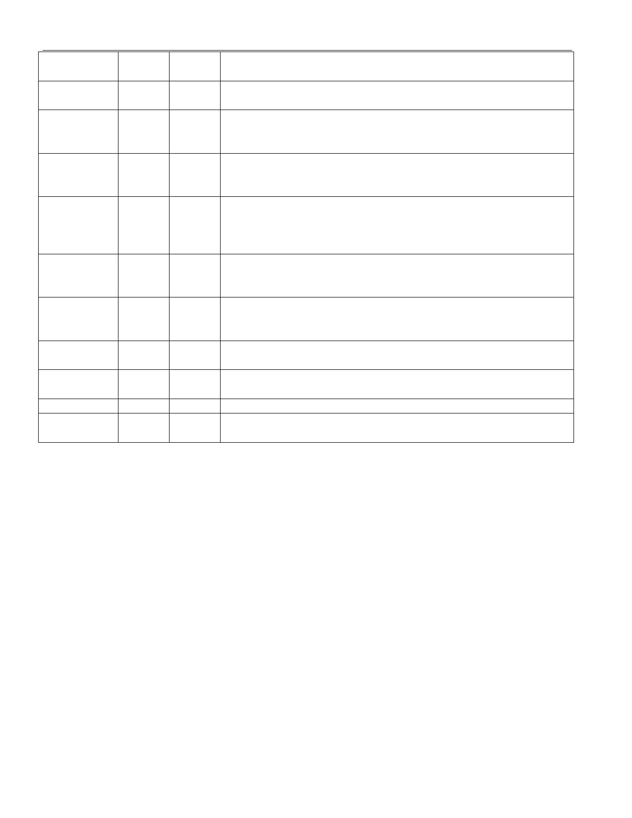
ACRONYM PIN I/O DESCRIPTION
DS2148/Q48
TCLK
43
I Transmit Clock. A 2.048 MHz or 1.544 MHz primary clock. Used
to clock data through the transmit side formatter.
TEST
26
I 3-State Control. Set high to 3-state all outputs and I/O pins
(including the parallel control port). Set low for normal operation.
Useful in board level testing.
TNEG
42
I Transmit Negative Data. Sampled on the falling edge (CES = 0) or
the rising edge (CES = 1) of TCLK for data to be transmitted out
onto the line.
TPD
13
I Transmit Power-Down.
0 = normal transmitter operation
1 = powers down the transmitter and 3-states the TTIP and TRING
pins
TPOS
41
I Transmit Positive Data. Sampled on the falling edge (CES = 0) or
the rising edge (CES = 1) of TCLK for data to be transmitted out
onto the line.
TTIP/
34/
O Transmit Tip and Ring [TTIP & TRING]. Analog line driver
TRING
37
outputs. These pins connect via a step-up transformer to the line. See
Section 7 for details.
TX0/
14/
I Transmit Data Source Select Bits 0 & 1 [H/W Mode]. These
TX1
15
inputs determine the source of the transmit data. See Table 4-6.
VDD
21/
- Positive Supply. 5.0V ±5%
36
VSM
20
I Voltage Supply Mode. Should be tied high for 5V operation
VSS
22/
- Signal Ground.
35
NOTES:
1) G.703 requires an accuracy of ±50ppm for both T1 and E1. TR62411 and ANSI specs require an
accuracy of ±32ppm for T1 interfaces.
2) * Denotes active low.
19 of 75
Share Link: 