CY7C106BN データシートの表示(PDF) - Cypress Semiconductor
部品番号
コンポーネント説明
一致するリスト
CY7C106BN Datasheet PDF : 8 Pages
| |||
CY7C106BN
CY7C1006BN
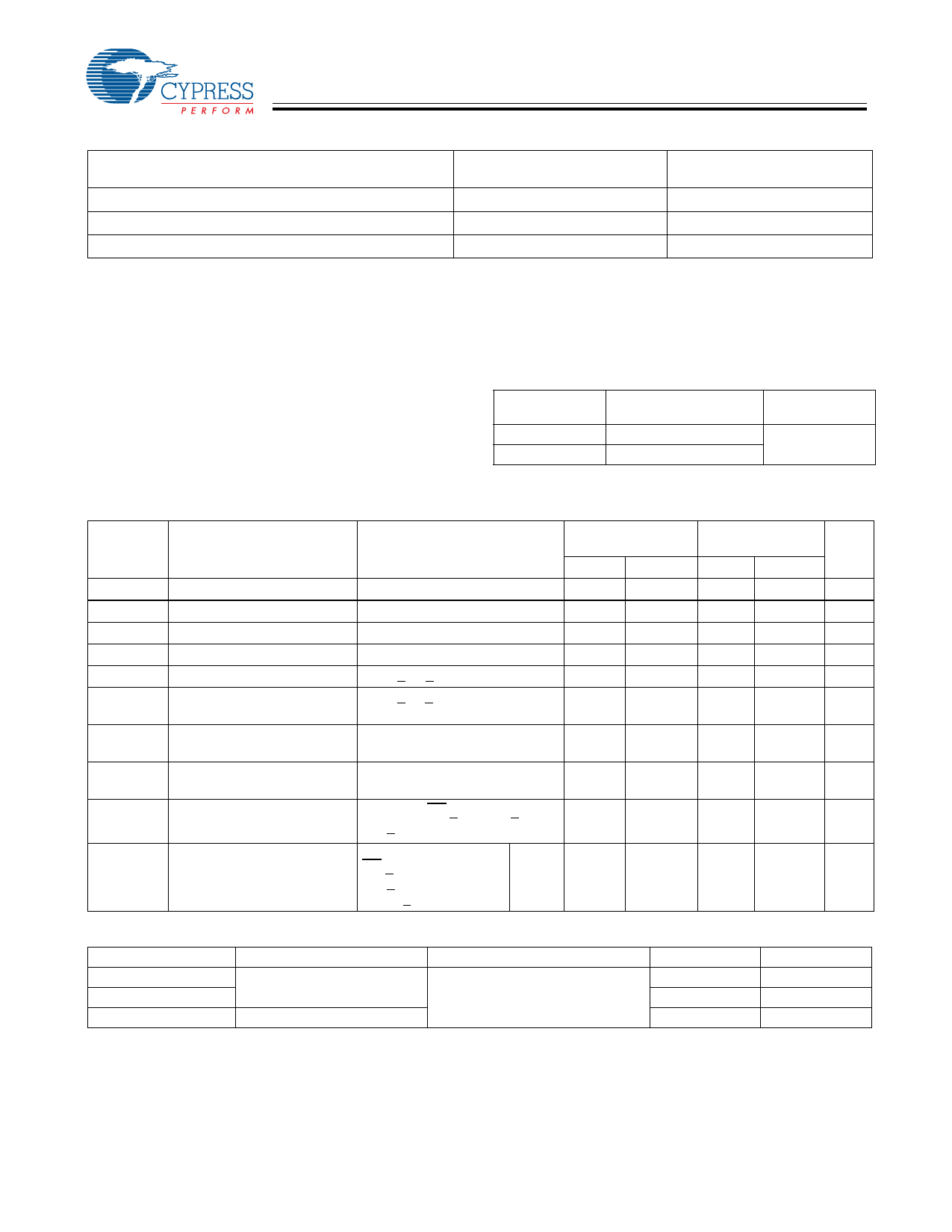
Selection Guide
Maximum Access Time (ns)
Maximum Operating Current (mA)
Maximum Standby Current (mA)
7C106BN-15
7C1006BN-15
15
80
30
7C106BN-20
7C1006BN-20
20
75
30
Maximum Ratings
(Above which the useful life may be impaired. For user guide-
lines, not tested.)
Storage Temperature ................................–65×C to +150×C
Ambient Temperature with
Power Applied............................................–55×C to +125×C
Supply Voltage on VCC Relative to GND[1] .... –0.5V to +7.0V
DC Voltage Applied to Outputs
in High Z State[1] ....................................–0.5V to VCC + 0.5V
DC Input Voltage[1].................................–0.5V to VCC + 0.5V
Current into Outputs (LOW)......................................... 20 mA
Static Discharge Voltage ........................................... >2001V
(per MIL-STD-883, Method 3015)
Latch-Up Current ..................................................... >200 mA
Operating Range
Range
Commercial
Industrial
Ambient
Temperature[2]
0°C to +70°C
–45°C to +85°C
VCC
5V ± 10%
Electrical Characteristics Over the Operating Range
Parameter
Description
VOH
Output HIGH Voltage
VOL
Output LOW Voltage
VIH
Input HIGH Voltage
VIL
Input LOW Voltage[1]
IIX
Input Leakage Current
IOZ
Output Leakage Current
IOS
Output Short
Circuit Current[3]
ICC
VCC Operating Supply
Current
ISB1
Automatic CE Power-Down
Current —TTL Inputs
ISB2
Automatic CE Power-Down
Current —CMOS Inputs
Test Conditions
VCC = Min., IOH = –4.0 mA
VCC = Min., IOL = 8.0 mA
GND < VI < VCC
GND < VI < VCC, Output
Disabled
VCC = Max., VOUT = GND
VCC = Max., IOUT = 0 mA,
f = fMAX = 1/tRC
Max. VCC, CE > VIH, VIN > VIH or
VIN < VIL, f = fMAX
Max. VCC,
CE > VCC – 0.3V,
VIN > VCC – 0.3V
or VIN < 0.3V, f=0
Com’l
7C106BN-15
7C1006BN-15
Min.
Max.
2.4
0.4
2.2 VCC + 0.3
–0.3
0.8
–1
+1
–5
+5
–300
80
30
10
7C106BN-20
7C1006BN-20
Min. Max. Unit
2.4
V
0.4
V
2.2 VCC + 0.3 V
–0.3
0.8
V
–1
+1
mA
–5
+5
mA
–300 mA
75
mA
30
mA
10
mA
Capacitance[4]
Parameter
Description
Test Conditions
CIN: Addresses
CIN: Controls
Input Capacitance
TA = 25×C, f = 1 MHz,
VCC = 5.0V
COUT
Output Capacitance
Notes:
1. VIL (min.) = –2.0V for pulse durations of less than 20 ns.
2. TA is the “instant on” case temperature.
3. Not more than 1 output should be shorted at one time. Duration of the short circuit should not exceed 30 seconds.
4. Tested initially and after any design or process changes that may affect these parameters.
Max.
7
10
10
Unit
pF
pF
pF
Document #: 001-06429 Rev. **
Page 2 of 8
[+] Feedback
Share Link: 