ACT6305 データシートの表示(PDF) - Active-Semi, Inc
部品番号
コンポーネント説明
一致するリスト
ACT6305 Datasheet PDF : 10 Pages
| |||
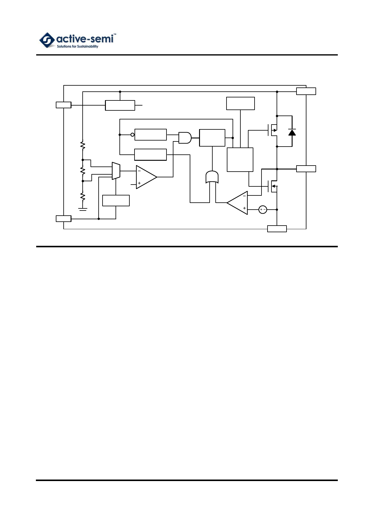
FUNCTIONAL BLOCK DIAGRAM
EN
REFERENCE
VREF
1µs
ONE -SHOT
5µs
ONE -SHOT
VREF
FEEDBACK
SELECT
ERROR
COMPARATOR
FB
ACT6305
Rev 3, 15-Nov-12
LOW INPUT
START UP
SET
LATCH Q
RESET
DRIVER
OUT
LX
CURRENT LIMIT
COMPARATOR
G
FUNCTIONAL DESCRIPTION
As seen in the Functional Block Diagram, the
ACT6305 comprises a reference, low input startup
circuitry, feedback select, error comparator, control
logic and timers, internal power MOSFETs and cur-
rent comparators.
Main Control Loop
The ACT6305 control architecture utilizes a series
of one-shot and current sense circuits to regulate
the output voltage with a very low quiescent supply
current of just 17µA. An ON cycle begins when FB
falls below the ACT6305’s internal reference volt-
age. During an ON cycle, the N-channel power
switch is turned on to connect the LX node to
ground, transferring energy from input supply to the
inductor. The ON cycle persists or the 1A current
limit is reached. When either of these conditions
occurs, the N-channel power switch turns off and
the OFF cycle begins. During the OFF cycle, the
energy stored in the inductor is released into the
output capacitor and load through the synchronous
rectifier. Once the 1µs minimum OFF time expires,
another ON cycle begins when the FB voltage
drops below the reference voltage.
Light Load Operation
Under light load conditions, the IC automatically
enters a power-saving mode by extending the OFF
time. This reduces switching losses and allows the
ACT6305 to maintain high efficiency across a very
wide load range.
Low Voltage Startup
The ACT6305 uses proprietary start-up circuitry that
allows it to achieve very low voltage startup down to
1V. The ACT6305 remains in low voltage startup
mode until VOUT exceeds 1.85V. The ACT6305 can-
not support its full rated load current when operat-
ing in low-voltage startup mode. Care should be
taken to minimize load current during startup.
Shutdown
In shutdown mode, all internal circuits including the
power switch and the synchronous rectifier are dis-
abled, reducing quiescent supply current to less
than 1µA. Note that in shutdown mode, a DC path
from the input supply to the output still exists due to
the body diode of the synchronous rectifier.
Innovative PowerTM
-7-
www.active-semi.com
Copyright © 2012 Active-Semi, Inc.
Share Link: 