ACT6305 データシートの表示(PDF) - Active-Semi, Inc
部品番号
コンポーネント説明
一致するリスト
ACT6305 Datasheet PDF : 10 Pages
| |||
ACT6305
Rev 3, 15-Nov-12
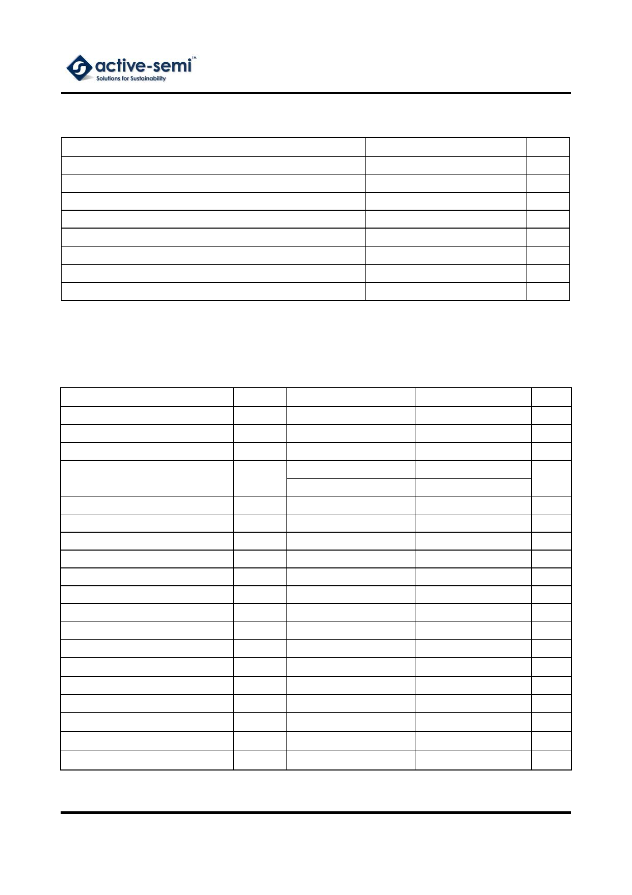
ABSOLUTE MAXIMUM RATINGSc
PARAMETER
VALUE
UNIT
OUT, EN to G
-0.3 to 6
V
FB, LX to G
Continuous LX Current
-0.3 to VOUT + 0.3
V
Internally Limited
A
Maximum Power Dissipation (derate 5mV/°C above TA = 50°C)
Junction to Ambient Thermal Resistance ( θJA )
Operating Junction Temperature
0.53
190
-40 to 150
W
°C/W
°C
Storage Temperature
-55 to 150
°C
Lead Temperature (Soldering, 10 sec)
300
°C
c: Do not exceed these limits to prevent damage to the device. Exposure to absolute maximum rating conditions for long periods may
affect device reliability.
ELECTRICAL CHARACTERISTICS
(VIN = 1.5V, VOUT = 3.3V, TA = 25°C, unless otherwise specified.)
PARAMETER
SYMBOL TEST CONDITIONS
Minimum Operating Input Voltage
Maximum Operating Input Voltage
Startup Voltage
VIN
VIN
VIN
ILOAD = 1mA
Output Voltage
VOUT
FB = OUT; 60mVPP Ripple
FB = G; 40mVPP Ripple
Output Voltage Range
External Feedback Divider
Quiescent Current at OUT
IQ
VFB = 1.3V
Shutdown Supply Current
ISD
EN = G
Startup to Normal Transition Threshold
FB Feedback Voltage
VFB
VOUT = 2V to 5V
FB Input Current
FB = 1.3V
Power Switch Current Limit
ILIM
Power Switch On Resistance
RONN ILX = 100mA
Synchronous Rectifier On Resistance
RONP ILX = -100mA
LX Leakage Current
EN = G, VLX = 0V or 3.3V
Maximum Switch On-Time
Minimum Switch Off-Time
tONMAX
tOFFMIN
EN Logic Low Threshold
VIL
EN Logic High Threshold
VIH
EN Input Current
MIN
3.2
4.85
2
1.15
0.7
3.75
0.75
0.6
TYP
0.6
1
3.3
5
17
0.1
1.85
1.180
50
1
0.19
0.21
0.1
5
1
MAX
5
1.18
3.4
5.15
5
34
1
1.21
1.25
0.4
0.4
1
6.25
1.25
0.3
1
UNIT
V
V
V
V
V
µA
µA
V
V
nA
A
Ω
Ω
µA
µs
µs
V
V
µA
Innovative PowerTM
-3-
www.active-semi.com
Copyright © 2012 Active-Semi, Inc.
Share Link: 