MT28S4M16LCTG-10 データシートの表示(PDF) - Micron Technology
部品番号
コンポーネント説明
一致するリスト
MT28S4M16LCTG-10 Datasheet PDF : 48 Pages
| |||
4 MEG x 16
SYNCFLASH MEMORY
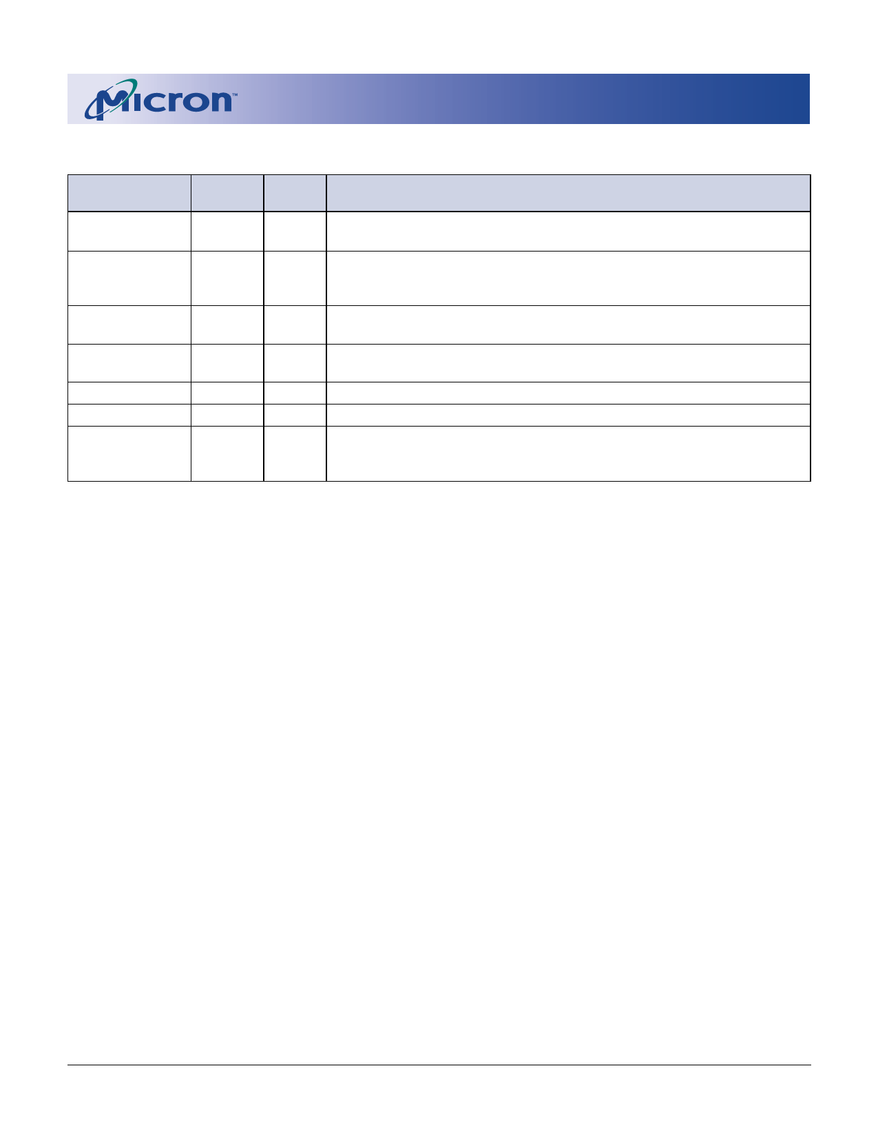
PIN DESCRIPTIONS (continued)
54-PIN TSOP
NUMBERS
20, 21
2, 4, 5, 7, 8, 10,
11,13, 42, 44, 45,
47, 48, 50, 51, 53
3, 9, 43, 49
6, 12, 46, 52
1, 14, 27
28, 41, 54
36
SYMBOL
BA0,
BA1
DQ0-
DQ15
VCCQ
VSSQ
VCC
VSS
VCCP
TYPE
Input
I/O
Supply
Supply
Supply
Supply
Supply
DESCRIPTION
Bank Address Input(s): BA0, BA1 define to which bank the command
is being applied. See Truth Tables 1 and 2.
Data I/O: Data bus.
DQ Power: Provide isolated power to DQs for improved noise
immunity.
DQ Ground: Provide isolated ground to DQs for improved noise
immunity.
Power Supply: 3.3V ±0.3V.
Ground.
Program/Erase Supply Voltage: VCCP must be tied externally to VCC. The
VCCP pin sources current during device initialization, PROGRAM and
ERASE operations.
4 Meg x 16 SyncFlash
MT28S4M16LC_6.p65 – Rev. 6, Pub. 9/01
6
Micron Technology, Inc., reserves the right to change products or specifications without notice.
©2001, Micron Technology, Inc.
Share Link: 